Dicing Saw (ADT): Difference between revisions
Jump to navigation
Jump to search
(Created page with "{{tool|{{PAGENAME}} |picture=SEM1.jpg |type = Packaging |super= Aidan Hopkins |phone= 805-893-3918x208 |location=Dicing Saw Room |email=hopkins@ece.ucsb.edu |description = ADT Di…") |
(Updated recipe recovery info) |
||
| (46 intermediate revisions by 6 users not shown) | |||
| Line 1: | Line 1: | ||
{{ |
{{tool2|{{PAGENAME}} |
||
|picture= |
|picture=ADT.jpg |
||
|type = Packaging |
|type = Packaging |
||
|super= |
|super= Lee Sawyer |
||
|super2= Aidan Hopkins |
|||
|phone= 805-893-3918x208 |
|||
|location= |
|location=Backend Lab: ESB 1111 |
||
|email=hopkins@ece.ucsb.edu |
|||
|description = ADT Dicing Saw |
|description = ADT Dicing Saw |
||
|model = ADT 7100 |
|||
|manufacturer = Advanced Dicing Technologies Ltd. |
|manufacturer = Advanced Dicing Technologies Ltd. |
||
|materials = |
|materials = |
||
|toolid=49 |
|||
}} |
}} |
||
= |
==About== |
||
The Model 7100 Series is a semi-automatic dicing saw. Semiconductor, glass, and plastic substrates of all types can be automatically or manually cut. This dicing Saw is optimized for multi-angle dicing of tight tolerance substrates up to 200 mm diameter in size. |
|||
Check the [https://wiki.nanotech.ucsb.edu/w/index.php?title=Packaging_Recipes#Dicing_Saw_Recipes_.28ADT_7100.29 Dicing Saw Recipes page] for the blades we currently stock. |
|||
=Dicing Seminar= |
|||
*[[Media:ADT-Applications.pdf|Applications]] |
|||
An ADT WM-966 tape applicator is used to mount samples to UV-release tape for dicing and an Ultron Systems UH104-8 UV lamp system is used to release samples post dicing. |
|||
*[[Media:ADT-Blade-Part1.pdf|Dicing Blade Technical Seminar - Part 1]] |
|||
*[[Media:ADT-Blade-Part2.pdf|Dicing Blade Technical Seminar - Part 2]] |
|||
Contact Staff for blades and dicing frames for your group. |
|||
*[[Media:ADT-Blade-Part3.pdf|Dicing Blade Technical Seminar - Part 3]] |
|||
*[[Media:ADT-Dressing.pdf|Dressing]] |
|||
==Detailed Specifications== |
|||
*[[Media:ADT-Dressing-Requirements.pdf|Dressing requirements & Instructions per Application]] |
|||
*[[Media:ADT-MagneticHeadDicingProcess.pdf|Magnetic Head Dicing Process]] |
|||
*Maximum Wafer Size: 8" |
|||
*[[Media:ADT-QNF-Singulation.pdf|QNF Singulation]] |
|||
*Parts mounted to UV-release tape for dicing |
|||
*[[Media:ADT-Troubleshooting.pdf|Troubleshooting]] |
|||
*Automated cut maps at multiple angles (0° and 90° typical) |
|||
*~Few micron alignment to on-wafer features. |
|||
*Thermocarbon Resnoid dicing blades provided by Staff |
|||
==Operating Procedures== |
|||
*[https://wiki.nanofab.ucsb.edu/w/images/5/54/ADT_SOP_Rev_J.pdf ADT Dicing Saw Standard Operating Procedure] |
|||
*[https://wiki.nanofab.ucsb.edu/w/images/5/5c/Post_Dicing_Tape_Expansion_SOP.pdf Post Dicing Tape Expansion] |
|||
*[https://wiki.nanofab.ucsb.edu/w/images/5/5a/Ultron_1042R_Film_specs.pdf Ultron Systems, Inc. 1042R Anti-Static Ultraviolet Film TDS] |
|||
*[https://wiki.nanofab.ucsb.edu/w/images/5/59/Recipe_Importing_New_Software.pdf Recovering an Old Recipe (2023)] |
|||
==Recipes== |
|||
*Recipes > Packaging > '''[[Packaging Recipes#Dicing Saw Recipes .28ADT 7100.29|Dicing Saw Recipes (ADT 7100)]]''' |
|||
Be sure to also see the recipes for protecting your sample from dicing dust, and mounting/unmounting. |
|||
Latest revision as of 17:55, 24 September 2024
| ||||||||||||||||||||||||||||||||
About
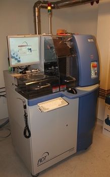
The Model 7100 Series is a semi-automatic dicing saw. Semiconductor, glass, and plastic substrates of all types can be automatically or manually cut. This dicing Saw is optimized for multi-angle dicing of tight tolerance substrates up to 200 mm diameter in size.
Check the Dicing Saw Recipes page for the blades we currently stock.
An ADT WM-966 tape applicator is used to mount samples to UV-release tape for dicing and an Ultron Systems UH104-8 UV lamp system is used to release samples post dicing.
Contact Staff for blades and dicing frames for your group.
Detailed Specifications
- Maximum Wafer Size: 8"
- Parts mounted to UV-release tape for dicing
- Automated cut maps at multiple angles (0° and 90° typical)
- ~Few micron alignment to on-wafer features.
- Thermocarbon Resnoid dicing blades provided by Staff
Operating Procedures
- ADT Dicing Saw Standard Operating Procedure
- Post Dicing Tape Expansion
- Ultron Systems, Inc. 1042R Anti-Static Ultraviolet Film TDS
- Recovering an Old Recipe (2023)
Recipes
- Recipes > Packaging > Dicing Saw Recipes (ADT 7100)
Be sure to also see the recipes for protecting your sample from dicing dust, and mounting/unmounting.
