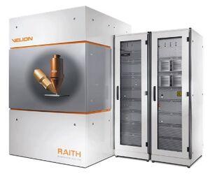
Focused Ion-Beam Lithography (Raith Velion): Difference between revisions
(added toolid, removed WIP, Pt dep/writing) |
mNo edit summary |
||
| Line 45: | Line 45: | ||
* Recipes > Lithography > '''[[Lithography Recipes#FIB Lithography Recipes .28Raith Velion.29|<u>FIB Lithography</u>]]''' |
* Recipes > Lithography > '''[[Lithography Recipes#FIB Lithography Recipes .28Raith Velion.29|<u>FIB Lithography</u>]]''' |
||
** ''Contains starting recipes etc.'' |
** ''Contains starting recipes etc.'' |
||
== Examples of FIB-SEM cross sections == |
|||
=== T-gates === |
|||
{| class="wikitable" |
|||
|+ |
|||
!''in situ'' SEM |
|||
!''ex situ'' SEM |
|||
|- |
|||
| |
|||
| |
|||
|} |
|||
=== Porous layers === |
|||
{| class="wikitable" |
|||
|+ |
|||
!''in situ'' SEM |
|||
!''ex situ'' SEM |
|||
|- |
|||
| |
|||
| |
|||
|} |
|||
== Example Images CHESSY == |
|||
{| class="wikitable" |
|||
|+ |
|||
! |
|||
! |
|||
! |
|||
! |
|||
|- |
|||
| |
|||
| |
|||
| |
|||
| |
|||
|- |
|||
| |
|||
| |
|||
| |
|||
| |
|||
|- |
|||
| |
|||
| |
|||
| |
|||
| |
|||
|} |
|||
Latest revision as of 01:57, 19 November 2024
|
About
VELION is a novel FIB-SEM instrument dedicated to advanced nanofabrication, in which FIB is the true priority technique. An evolution of Raith’s ionLINE, the ion column at the vertical position features a unique design to meet the most demanding nanofabrication requirements. It is supported by a field emission SEM solution as well as a highest-precision laser interferometer-controlled sample stage.
With its FIB-prioritized nanofabrication setup, including SEM and a high-accuracy stage, VELION allows for versatile use in four different operation modes that offer
• direct and versatile FIB patterning for simplified, flexible, 3D, and automated processing
• highest-precision nanofabrication over extended areas and periods of time with both FIB and SEM
• SEM imaging for in-situ process control, inspection and sample preparation.
The Raith Velion ion beam tool was installed at UCSB in 2020 and signed off and avaiable for. use in early 2021.
Detailed Specifications
nanoFIB column:
- Liquid Metal Alloy Ion Sources (LMAIS) providing ions for Gallium-free patterning (Au, Si)
- High resolution patterning capabilities (minimum feature size < 15nm)
- Fully corrected write fields (distortion, stigmation)
- Long term current stability (days)
Laser Interferometer stage:
- Mechanical movement at 1nm precision
- Continuous stage modes for stitch free FIB patterning on full 4”wafer scale
- Stitching and overlay accuracy: < 50 nm ( mean+3 sigma)
FE SEM
- Process control for rapid prototyping
Additional Capabilities:
- Automated height sensing to detect sample surface height variation for automated correction
- Pt Gas Injection System (GIS) localized deposition/writing
- Raith Nanosuite software including CAD (GDSII) navigation & patterning
Recipes
- Recipes > Lithography > FIB Lithography
- Contains starting recipes etc.
Examples of FIB-SEM cross sections
T-gates
| in situ SEM | ex situ SEM |
|---|---|
Porous layers
| in situ SEM | ex situ SEM |
|---|---|
