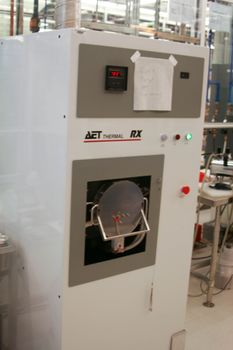
Rapid Thermal Processor (AET RX6): Difference between revisions
| (9 intermediate revisions by 5 users not shown) | |||
| Line 1: | Line 1: | ||
{{ |
{{tool2|{{PAGENAME}} |
||
|picture=RTP.jpg |
|picture=RTP.jpg |
||
|type = Vacuum Deposition |
|type = Vacuum Deposition |
||
|super= |
|super= Bill Millerski |
||
|super2= Tony Bosch |
|||
|phone=(805)839-3918x210 |
|phone=(805)839-3918x210 |
||
|location=Bay 3 |
|location=Bay 3 |
||
| Line 11: | Line 12: | ||
|toolid=42 |
|toolid=42 |
||
}} |
}} |
||
= |
=About= |
||
Our rapid thermal annealer is manufactured by AET. Heating is achieved through two banks of heat lamps that deliver optical energy through the all-quartz chamber. With this unit, atmospheric pressure anneals in Oxygen, Nitrogen and Forming Gas can be done to temperatures up to 1200°C for three minutes. An inner liner is used to prevent contamination to the main quartz chamber. A thermocouple and pyrometer are available for maintaining temperature control. The system can hold one 4-inch wafer or smaller substrates placed on top of a Silicon carrier wafer. Custom windows based control software has been added to the system by Sedona Visual Controls. All process parameters are monitored and stored. Typical anneals are done for: ohmic contact formation to semiconductors, implant activation, damage annealing, dopant activation, and film densification. A variety of materials can be annealed in the chamber, including Si, SiO<sub>2</sub>, Si<sub>3</sub>N<sub>4</sub>, GaAs, InP, GaSb, GaN, and metals. For materials that will decompose at the elevated temperatures, a dielectric anneal cap must be deposited on the wafer or an enclosed wafer holder must be used to prevent contamination of the chamber walls. |
Our rapid thermal annealer is manufactured by AET. Heating is achieved through two banks of heat lamps that deliver optical energy through the all-quartz chamber. With this unit, atmospheric pressure anneals in Oxygen, Nitrogen and Forming Gas can be done to temperatures up to 1200°C for three minutes. An inner liner is used to prevent contamination to the main quartz chamber. A thermocouple and pyrometer are available for maintaining temperature control. The system can hold one 4-inch wafer or smaller substrates placed on top of a Silicon carrier wafer. Custom windows based control software has been added to the system by Sedona Visual Controls. All process parameters are monitored and stored. Typical anneals are done for: ohmic contact formation to semiconductors, implant activation, damage annealing, dopant activation, and film densification. A variety of materials can be annealed in the chamber, including Si, SiO<sub>2</sub>, Si<sub>3</sub>N<sub>4</sub>, GaAs, InP, GaSb, GaN, and metals. For materials that will decompose at the elevated temperatures, a dielectric anneal cap must be deposited on the wafer or an enclosed wafer holder must be used to prevent contamination of the chamber walls. |
||
= |
=Detailed Specifications= |
||
*Maximum ramp rate of 50°C/Sec. |
|||
*Temperatures of 1000°C for 20 min., 1100°C for 5 min., 1200°C for 1 min. Oxygen, Nitrogen and Forming Gas flows up to 10LPM. TC use for anneals up to 1200°C |
|||
*Oxygen, Nitrogen and Forming Gas flows up to 10LPM. |
|||
*TC use for anneals up to 1200°C |
|||
*Windows-based process monitoring and control software by Sedona Visual Controls |
*Windows-based process monitoring and control software by Sedona Visual Controls |
||
'''Max temp vs time:''' |
|||
| ⚫ | |||
| ⚫ | |||
*1200°C for 3 min |
|||
| ⚫ | |||
*[https://wiki.nanotech.ucsb.edu/w/images/0/0b/RTA_AET_Operating_Instructions.pdf Operating Instuctions] |
|||
{| border="1" class="wikitable" style="border: 1px solid #D0E7FF; background-color:#ffffff; text-align:center;" |
|||
|- |
|||
|width="100"|Temperature||width="75"|Time |
|||
|- |
|||
| ⚫ | |||
|- |
|||
|1100°C||10 min |
|||
|- |
|||
| ⚫ | |||
|- |
|||
|1300°C|| 10 sec |
|||
|- |
|||
|} |
|||
| ⚫ | |||
*[[media:AET RTA Operating Instructions.pdf|Operating Instuctions]] |
|||
Latest revision as of 19:33, 14 March 2025
| ||||||||||||||||||||||||||||||
About
Our rapid thermal annealer is manufactured by AET. Heating is achieved through two banks of heat lamps that deliver optical energy through the all-quartz chamber. With this unit, atmospheric pressure anneals in Oxygen, Nitrogen and Forming Gas can be done to temperatures up to 1200°C for three minutes. An inner liner is used to prevent contamination to the main quartz chamber. A thermocouple and pyrometer are available for maintaining temperature control. The system can hold one 4-inch wafer or smaller substrates placed on top of a Silicon carrier wafer. Custom windows based control software has been added to the system by Sedona Visual Controls. All process parameters are monitored and stored. Typical anneals are done for: ohmic contact formation to semiconductors, implant activation, damage annealing, dopant activation, and film densification. A variety of materials can be annealed in the chamber, including Si, SiO2, Si3N4, GaAs, InP, GaSb, GaN, and metals. For materials that will decompose at the elevated temperatures, a dielectric anneal cap must be deposited on the wafer or an enclosed wafer holder must be used to prevent contamination of the chamber walls.
Detailed Specifications
- Maximum ramp rate of 50°C/Sec.
- Oxygen, Nitrogen and Forming Gas flows up to 10LPM.
- TC use for anneals up to 1200°C
- Windows-based process monitoring and control software by Sedona Visual Controls
Max temp vs time:
- 1000°C for 20 min
- 1100°C for 5 min
- 1200°C for 3 min
