Molecular Vapor Deposition: Difference between revisions
Jump to navigation
Jump to search
Content deleted Content added
Text replacement - "www.nanotech.ucsb.edu/wiki/" to "wiki.nanotech.ucsb.edu/wiki/" |
→Recipes: link to new process traveler |
||
| Line 21: | Line 21: | ||
*[https://signupmonkey.ece.ucsb.edu/wiki/images/f/f4/MVD_SOP.pdf MVD Standard Operating Procedure] |
*[https://signupmonkey.ece.ucsb.edu/wiki/images/f/f4/MVD_SOP.pdf MVD Standard Operating Procedure] |
||
*[[MVD - Wafer Coating - Process Traveler|Wafer Coating - Process Traveler]] |
|||
Revision as of 17:15, 23 July 2020
| ||||||||||||||||||||
About
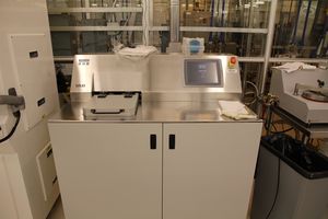
The Molecular Vapor deposition system is used for deposition of a monolayer-thick fluorocarbon film for producing extremely hydrophobic surfaces used for anti-sticking layers for nanoimprinting or anti-stiction layers for MEMS. The system has integrated Oxygen plasma cleaning for organic removal and surface activation and can be run at temperatures up to 80°C. Multi-step recipes can be created. The system is currently configured for FDTS (perflourodecyltricholorsilane) and water to producing the coatings. Up to 6” wafers can be coated in the system.
Recipes
- Nanoimprinting recipes using FDTS non-stick layer
- MVD Standard Recipes
