Photoluminescence PL Setup (Custom): Difference between revisions
Jump to navigation
Jump to search
Content deleted Content added
→Pump Lasers Available: added 532nm laser |
supervisor = Demis |
||
| Line 2: | Line 2: | ||
|picture=Holograph.jpg |
|picture=Holograph.jpg |
||
|type = Inspection, Test and Characterization |
|type = Inspection, Test and Characterization |
||
|super= |
|super= Demis D. John |
||
|phone=(805) 839-5689 |
|||
|location=Bay 6 |
|location=Bay 6 |
||
|email=Ningcao@ece.ucsb.edu |
|||
|description = Custom Built Photoluminescence |
|description = Custom Built Photoluminescence |
||
}} |
}} |
||
Revision as of 03:45, 27 September 2023
|
About
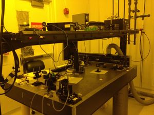
The Photoluminescence setup is on the same optical table as the Hologaphic Lithography setup.
This custom setup is used for materials characterization including crystal growth quality and gain region/quantum well growth, or semiconductor alloy ratio. Multiple laser sources are available - including the He-Cd laser also used for Holography, via a flip-down mirror.
Light is delivered in free-space, selected via magnetic flip-mirrors, and collected by optical fiber, and analyzed by a USB spectrometer.
Detailed Specifications
Pump Lasers Available
- 325nm He-Cd - single mode, spatially filtered
- 405nm Diode Laser
- 532nm Diode Laser
- 657nm Diode Laser
Optical Detection
- Ocean Optics USB2000+
- 340nm to 1025nm wavelength acquisition, through multi mode optical fiber
- Raman spectrometer
