E-Beam 4 (CHA): Difference between revisions
No edit summary |
updated pics and added pic of controls |
||
| Line 12: | Line 12: | ||
|materials = |
|materials = |
||
|toolid=10 |
|toolid=10 |
||
}} |
}} |
||
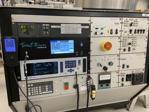
[[File:EBeam4 Controls.jpeg|thumb|EBeam4's controls]] |
|||
| ⚫ | |||
| ⚫ | |||
This electron-beam evaporation system is a bell-jar type system and has the capability to do up to 9-4” wafers in a lift-off configuration and up to 18-4” wafers in a sidewall coverage configuration. Rotational motion in combination with baffling is used for lift-off and provides roughly 5% uniformity across a 4” wafer. The sidewall coverage fixturing uses full planetary motion to provide coverage over all sidewalls. The system also an 8-pocket e-beam source and an Inficon IC/5 deposition controller that allows for programming of fully automated multiple layer depositions. The metals available for deposition are Al, Ti, Au, Pt, Ni, Pd, Ag, Ge, Fe, NiCr, NiFe and Cr. This system is used for n-type ohmic contact metalization to compound semiconductors, Schottky contacts to semiconductors, bond pads, and other general metalizations. The maximum deposition thickness during a run is limited to 1.0 microns. |
This electron-beam evaporation system is a bell-jar type system and has the capability to do up to 9-4” wafers in a lift-off configuration and up to 18-4” wafers in a sidewall coverage configuration. Rotational motion in combination with baffling is used for lift-off and provides roughly 5% uniformity across a 4” wafer. The sidewall coverage fixturing uses full planetary motion to provide coverage over all sidewalls. The system also an 8-pocket e-beam source and an Inficon IC/5 deposition controller that allows for programming of fully automated multiple layer depositions. The metals available for deposition are Al, Ti, Au, Pt, Ni, Pd, Ag, Ge, Fe, NiCr, NiFe and Cr. This system is used for n-type ohmic contact metalization to compound semiconductors, Schottky contacts to semiconductors, bond pads, and other general metalizations. The maximum deposition thickness during a run is limited to 1.0 microns. |
||
= |
=Detailed Specifications= |
||
*Temescal 10kV power supply |
*Temescal 10kV power supply |
||
*1-Temescal 8-pocket series 260 e-beam sources |
*1-Temescal 8-pocket series 260 e-beam sources |
||
| Line 29: | Line 32: | ||
=Documentation= |
=Documentation= |
||
*[https://wiki.nanotech.ucsb.edu/w/images/8/8b/Wiki_Operational_Procedure_EB4_With_EBC_Rev_3.pdf Operating Procedures] |
*[https://wiki.nanotech.ucsb.edu/w/images/8/8b/Wiki_Operational_Procedure_EB4_With_EBC_Rev_3.pdf Operating Procedures] |
||
= |
=Materials Table= |
||
For the materials tables, please visit the [[E-Beam_Evaporation_Recipes#Materials_Table_(E-Beam #4)|E-Beam Recipe Page]]. |
For the materials tables, please visit the [[E-Beam_Evaporation_Recipes#Materials_Table_(E-Beam #4)|E-Beam Recipe Page]]. |
||
Revision as of 19:17, 8 September 2022
| ||||||||||||||||||||||||||||||||

About
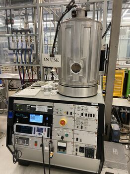
This electron-beam evaporation system is a bell-jar type system and has the capability to do up to 9-4” wafers in a lift-off configuration and up to 18-4” wafers in a sidewall coverage configuration. Rotational motion in combination with baffling is used for lift-off and provides roughly 5% uniformity across a 4” wafer. The sidewall coverage fixturing uses full planetary motion to provide coverage over all sidewalls. The system also an 8-pocket e-beam source and an Inficon IC/5 deposition controller that allows for programming of fully automated multiple layer depositions. The metals available for deposition are Al, Ti, Au, Pt, Ni, Pd, Ag, Ge, Fe, NiCr, NiFe and Cr. This system is used for n-type ohmic contact metalization to compound semiconductors, Schottky contacts to semiconductors, bond pads, and other general metalizations. The maximum deposition thickness during a run is limited to 1.0 microns.
Detailed Specifications
- Temescal 10kV power supply
- 1-Temescal 8-pocket series 260 e-beam sources
- Cryo-pumped system with ~ 5e-7 ultimate base pressure
- Rotation with baffle for 5% uniformity over 4” wafer
- Automatic vacuum sequencing
- Temescal e-beam sweep control
- Inficon IC/5 programmable crystal thickness monitoring system
- Automatic deposition of multiple layer stacks
- Sample size: Pieces or up to 10-4” wafers for lift-off and 24-4” wafers for sidewall coverage
- Metals: Al, Ti, Au, Pt, Ni, Pd, Ag, Ge, Fe, NiCr, NiFe, Cr
Documentation
Materials Table
For the materials tables, please visit the E-Beam Recipe Page.
