DSEIII (PlasmaTherm/Deep Silicon Etcher): Difference between revisions
No edit summary |
Freeborn d (talk | contribs) |
||
| Line 38: | Line 38: | ||
==Operation Procedures & Documentation== |
==Operation Procedures & Documentation== |
||
*{{file|DSEIII Operating Instructions.pdf |
*{{file|DSEIII Operating Instructions.pdf}https://wiki.nanotech.ucsb.edu/wiki/File:Running_a_process.pdf |
||
*[[Laser Etch Monitoring|Laser Etch Monitoring procedures]] |
*[[Laser Etch Monitoring|Laser Etch Monitoring procedures]] |
||
| Line 50: | Line 50: | ||
'''Remove at least 7mm around ALL of the outer edge of the 4-inch wafer. Do not try to save die by removing less, or you will lose the whole wafer and require the chamber to be vented.''' |
'''Remove at least 7mm around ALL of the outer edge of the 4-inch wafer. Do not try to save die by removing less, or you will lose the whole wafer and require the chamber to be vented.''' |
||
Pieces of wafers can be placed onto 4" silicon wafers, or mounted as long as material does not get on the clamp. It is common for through-silicon etches to use a carrier wafer, often bonded with wax on the [[Wafer Bonder (Logitech WBS7)|Logitech bonder]], and excess wax carefully removed to ensure not adhesion to the clamp. |
Pieces of wafers can be placed onto 4" silicon wafers, or mounted as long as material does not get on the clamp. It is common for through-silicon etches to use a carrier wafer, often bonded with wax on the [[Wafer Bonder (Logitech WBS7)|Logitech bonder]], and excess wax carefully removed to ensure not adhesion to the clamp. |
||
==Recipes== |
==Recipes== |
||
Revision as of 23:42, 14 September 2022
| ||||||||||||||||||||||||||||||
About
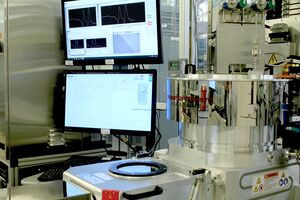
The Si DRIE system is a Plasma-Therm DSEIII series system with a loadlock. The system has an Inductively Coupled Plasma (ICP) coil and a capactively coupled substrate HF (13.56MHz) and LF (100kHz) supplies to independently control plasma density and ion energy in the system. This system is dedicated to deep silicon Bosch etching, although short O2 etches are also permitted. The fixturing is configured for 4" diameter Si wafers and uses a clamp to hold the sample on the RF chuck.
The materials allowed to be exposed in the system are limited to Silicon, SiO2, Si3N4, SiOXNY, and polymer films such as photoresist, PMMA, and polyimide. Other materials can be placed in the chamber with staff approval.
Helium back-side cooling is used to keep the sample cool during the etch. Temperature control is very important as the polymer passivation layer is chemically etched away by the fluorine gas at elevated temperatures, resulting in loss of profile control.
The etch rate is dependent on the open area of silicon (macro-loading effect) with large open area samples etching slower than small open area samples. Features with a high aspect ratio will also etch slower than more open areas. This is known as RIE lag or the micro-loading effect.
The in-situ laser monitor installed on this system allows for repeatable etches and endpoint detection via continuous optical monitoring of the wafer reflectivity in a user-determined location, through a porthole on the chamber.
Detailed Specifications
- 3500 W ICP coil power at 2 MHz and 500 W substrate bias at 13.56 MHz plasma generators
- C4F8, SF6, O2, Ar, N2 gases available
- He-back-side cooling
- 100mm wafer held down with ceramic clamp., single-load
- Users must ensure thick photoresists or other substances do not contact the clamp, to prevent wafer stiction and breakage.
- Windows-based Cortex software control of process and wafer handling
- Allowed materials: Silicon, SiO2, Si3N4, SiOXNY, Al, Al2O3, and polymer films such as photoresist, PMMA, and polyimide; CrystalBond wax for mounting to carrier wafer (ask staff before using oil).
- Realized etch rates (including passivation steps) for Bosch process of >8 um / min. Selectivity to resist > 80:1 for low aspect ratio.
- Laser monitoring with camera and etch simulation software: Intellemetrics LEP 500
Operation Procedures & Documentation
- {{file|DSEIII Operating Instructions.pdf}https://wiki.nanotech.ucsb.edu/wiki/File:Running_a_process.pdf
- Laser Etch Monitoring procedures
Preventing Wafer Breakage
It is very important that your wafer does not stick to the top-side clamp in the chamber. The clamp will get hot during long etches, causing thick photoresists to soften and adhere to the clamp, resulting if wafer loss and breakage.
Users must remove photoresist from the wafer edge to prevent this. We have photolithographic methods for performing this cleanly, or simple swabbing with EBR100 also works well.
See this page for Edge-Bead Removal techniques: Manual Edge-Bead Removal Techniques
Remove at least 7mm around ALL of the outer edge of the 4-inch wafer. Do not try to save die by removing less, or you will lose the whole wafer and require the chamber to be vented.
Pieces of wafers can be placed onto 4" silicon wafers, or mounted as long as material does not get on the clamp. It is common for through-silicon etches to use a carrier wafer, often bonded with wax on the Logitech bonder, and excess wax carefully removed to ensure not adhesion to the clamp.
Recipes
- Plasma-Therm DSE-iii Recipes - Recipes specific to this tool.
- All Dry Etching Recipes - use this list to see other options for dry etching various materials.
- Online Training Video:
- Plasmatherm DSE-iii Training
- Important: This video is for reference only, and does not give you authorization to use the tool. You must be officially authorized by the supervisor before using this machine.
