MLA150 - Troubleshooting: Difference between revisions
→Causes: added OAF driving off wafer |
→Solutions for small substrates: --> sols for ALL substrate types |
||
| Line 23: | Line 23: | ||
#Very dark (low reflection) areas of the wafer can also cause the OptAF surface detection to lose signal, and lose the feedback signal needed to maintain focus during a write. |
#Very dark (low reflection) areas of the wafer can also cause the OptAF surface detection to lose signal, and lose the feedback signal needed to maintain focus during a write. |
||
===Solutions for |
===Solutions for all substrate types=== |
||
For Samples that are less than ~1 or 2 inches, try the following methods (listed with most effective first): |
For Samples that are less than ~1 or 2 inches, try the following methods (listed with most effective first): |
||
Revision as of 17:59, 5 June 2024
Look below for the issue you're experiencing, to see if we have a workaround or solution.
Make sure you record your problem and solution in the log book! This is very important for allowing us to improve system stability and make repairs.
Unexpected Behavior
- If the software is acting unusual (eg. black screen), or stage is moving to an incorrect location, or Convert software unable to launch, it could be due to the computer running out of RAM memory.
- A computer restart typically resolves this. Run the restart procedure further down this page to resolve.
- If you're seeing unexpected stopping of the exposure, either right at the beginning of the exposure, or in the middle (after clicking [Start Exposure]), then the Design file may have become corrupted. Designs are prone to corruption if aborted partway through an exposure/conversion.
- Re-import your original GDS/BMP/DXF file in the [Convert Design] screen to try to resolve this.
Out Of Focus Exposures
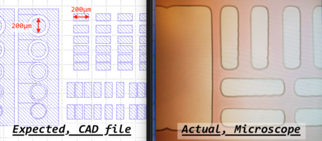
After developing, you find that some of all of your pattern is extremely out of focus. Small features (less than ~100µm) don't show up at all, and large features are extremely rounded, sometimes with rainbows at the PR edges indicating extremely slanted photoresist.

Causes
There are multiple possible causes for this issue:, all of which have to do with the Optical Autofocus' confocal surface detection:
- The Optical AutoFocus laser is starting the write on an extremely non-uniform part of the photoresist spin (eg. corner of quarter-wafer), which causes it to drive out of focus before the write starts.
- The Optical Autofocus driving off/onto a round wafer can also cause it to go out of focus during the write, with no warnings (it'll keep exposing).
- Very dark (low reflection) areas of the wafer can also cause the OptAF surface detection to lose signal, and lose the feedback signal needed to maintain focus during a write.
Solutions for all substrate types
For Samples that are less than ~1 or 2 inches, try the following methods (listed with most effective first):
- Before starting the exposure: Enable the Low/High Mag microscope (NOT Overview camera), and move the scope to a “good”/uniform region of the sample before hitting [Start Exposure]. Make sure the sample features (or dirt/defects) are in-focus, indicating that the OptAF is correctly tracking the surface. The system will perform an initial re-focus in this location right before beginning the exposure.
- Make sure the High/Low Res (not overview) camera is on a uniform area of the sample before hitting [Start Exposure].
- Make sure the ORIGIN (0,0) coordinate of your CAD file is placed in a relatively uniform area of your sample. Do not place the Origin at the corner or on PR edge-bead, as the Optical AF laser may do an initial measurement at this location. If you are trying to align your die to a corner, use this technique instead.
- Remove thick photoresist edge-bead prior to exposure (eg. with razor blade, or a little EBR100 on a cotton swab). Some edge-bead removal techniques: Photolithography - Manual Edge-Bead Removal Techniques
Solution for 3-4 inch wafers
- Adjust your design/CAD file so the design is about ≥10mm from the edges of the wafer (in the Y direction especially) has been reported to help. The write-head overtravels past the CAD design by ~8-9mm, so this can prevent the head from hitting the PR edge-bead/wafer-edge (the cause of focus-loss).
- Try removing the edge-bead of your PR: Photolithography - Manual Edge-Bead Removal Techniques
- For large substrates, switching to Pneumatic Autofocus works well (although focus repeatabiity is less stable, eg. focus shifts by ±5 over a few weeks). PneuAF causes a few-mm of edge-bead area to expose out-of-focus, which is acceptable for full-wafers, but often too large exclusion for smaller samples.
- Contact the supervisor for info on switching to Pneumatic AF. Do NOT use PneuAF without first asking Staff! There is significant crash potential if performed incorrectly.
- PneuAF will usually have a slightly different defocus offset compared to OptAF. You should run a new FEM/Series with PneAF.
- PneuAF will require Focus/Exposure calibration (in Series mode) more often than OptAF.
Debugging
After exposure, open the logfile for your Job (see this tip for logfile location) and search for the word "piezo". This records the Z-height Piezo position - the physical autofocus position - at the end/start of each stripe (when the optical head changes direction, off the substrate). Since the piezo freezes motion off the substrate, this value indicates the autofocus piezo height at the edge of your substrate.
When in-focus on your substrate this should be in the range ~2,000 to 25,000 or so. If you see a value like "192" or <500, then this usually means the autofocus drove to it's limit, because it was not tracking the substrate surface. Sometimes the first one or two stripes are in-focus, and then the rest are out of focus. Other times, the system is out of focus from the start, and stays this way for the entire exposure.
You can see the optical autofocus laser position in the camera, it is about 6µm up-left from the central crosshair. It is a confocal surface detection, which continuously tracks the surface – even while manually driving around the substrate before exposure. When this laser hits a bad point (eg. black /dark no reflection, or particle, or steep slope) it can lose surface tracking. During substrate load, the system attempts to land on the surface using this system.
Before exposure, if you see your surface is far out of focus, then your exposure will likely also be out of focus (the same continuous AutoFocus is active during microscope imaging).
- Try un/re-loading the substrate, and alter the substrate position
- Make sure there are no black/very dark spots on the substrate which would cause the system to be unable to optically detect the surface
- For transparent, thin substrates, try switching to blanket deposition and etching (instead of liftoff), to provide an opaque surface
- If nothing else works, use contact alignment with a photomask.
Exposure Logs / Reports
- You can find a detailed log file of each exposure in the folder
C:\HIMT\LogFiles\ExposureLogs. At the end of this file you can find final statistics from Field (Local) Alignment. You can copy the appropriate log file into your Nanofiles user folder to make it accessible via FTP. - If you run into an unusual error, please let us know the Job Name, so that we can locate this log file if needed.
- You can find a detailed log file of each exposure in the folder
Stitching
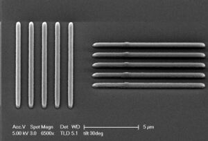
The system raster scans the ~12x20µm exposure fields across the wafer, and there will be stitching errors at the boundaries.
The "fast-scan" axis is in ±Y, which causes the largest stitching errors to show up as Y-oriented stripes, ridges or bumps, every ~20µm in X. We estimate that these ridges indicate about 4-7% lower dose at the stitching boundary.
When you are fully-exposing your PR (typically with a bit of over-exposure, eg. ~20% overdose), these stitching boundaries are barely visible, if at all, and typically correspond to a ~50nm bump in the feature.
However for partially-exposed PR (such as in grey-scale exposure), these ridges will clearly manifest as Y-oriented ridges of ~4-7% lower exposure dose, and reduced underexposed PR.

Overexposing the design can reduce the size of these stitching bumps. Since that will also alter your feature size on-wafer, you can us the Convert correction "CD Bias" to correct your feature sizes accordingly, see this page for more info on using that option. Or just adjust your exposure CAD file feature sizes accordingly.
Stage not centered during [Substrate Load]
When the system moves the stage to place your sample under the lens, the center of the stage is not under the lens!
WARNING: Do NOT continue if this occurs - there is significant danger of crashing the lens into a sample.
- Cancel the substrate load process.
Workaround
- In the software Menu, choose Tools > Initialize Stage, then retry your Job.
- If that does not solve the problem, please reboot the computer (instructions below), which will also reinitialize all motor controllers.
Note: if you chose a “Small” substrate template, the system always moves the sample under the overview camera at first, which is the the Left of the main write head. You’ll see the yellow microscope illumination around your sample. This is normal behavior.
Defocus: unable to enter ±25 full range
In the Setup screen, Editors for Resist or Series templates, you are limited to only ±10 defocus, even though the system is capable of ±25.
Workaround
- During Job Setup, make sure to choose "_General-Focus". User-made Resist templates usually won't have the setting correctly applied, unless they copied a Staff resist.
- In the Exposure screen - after wafer load etc. - you may still edit the defocus range, and in this screen you are able to type in the full range ±25. For a Series exposure (focus-exposure matrix, FEM), you can choose the "_Manual" template during Setup, and on the Expose screen you can edit the Series array to your needs with full defocus range.
Convert software is unable to launch
- Check whether the XWindows software is available in the Windows Start bar - sometimes the window lands behind the MLAMenu software.
- If an error window is indicating some error with launching convert, then perform the computer reboot procedure below.
Focus Depth Motor Not Initialized
After an exposure has been initiated, but before exposure has actually begun, you get an error window stating the the "Focal Depth Motor is not initialized."
Notify staff
We can reinitialize that motor remotely, which will allow you to start your exposure.
Nanofiles folder not showing up on SFTP
Problem: When you log into the Nanofiles FTP server, you don't see an "MLA_Heidelberg" folder to upload your CAD files.
Reason: After your user's folder is created in the Users_Nanofiles folder on the MLA computer, our FTP server only creates the corresponding folder on the Nanofiles FTP site once per day around 00:00 midnight.
Wait until the next morning and your folder should be available. If you need immediate access, please email the tool supervisors, and one of us can upload your file into our Staff folder on the tool.
You can find more troubleshooting info about the Nanofiles FTP at the corresponding Frequently Asked Questions section.
Aligning to a quarter-wafer/irregular piece
For alignment of your die to a quarter-wafer, one accurate method for accounting for both rotation and die placement is to
use 2nd Layer / Manual Alignment with 2 coordinates to align to the wafer's flat edge.

Detailed procedure is as follows:
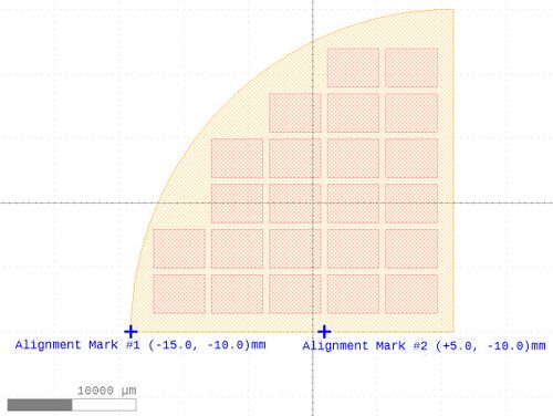
- Set up your CAD file with a mock-up of the quarter wafer on a construction Layer, and align your die (on a production Layer) to this. The quarter-wafer should have a flat edge "down" (negative Y).
- Make sure the Origin (0,0) of your CAD file is in a uniform region of your quarter wafer- ie. not on the edge/edge-bead/non-uniform photoresist.
- Determine coordinates to two points along the the Bottom edge of the quarter-wafer.
- On the MLA, use "2nd layer" exposure, enabling alignment.
- Use the "Rectangular" substrate template (Usually "_Rectangular_OptAF")
- Load your quarter-wafer according to your CAD file, with a flat-edge "down" (–Y).
- Type in the two coordinates to the pretend alignment marks along the wafer bottom.
- On the [Alignment] screen, click [Move to First Mark]
- If you need to move the stage to see the wafer edge, move only in Y (up/down), don't move left/right. If you make a mistake, click [Move to First Mark] again.
- Change the Alignment dropdown list from "CrossAlignment" --> "Manual"
- Choose High or Low magnification on the microscope. (High will be more accurate.)
- Click [Measure], and the system will ask you to click on the alignment mark on the video window.
- Click on the wafer edge, but directly above/below the screen's central crosshair - so we're only correcting the Y-coordinate. The mouse crosshair's Y-axis should line up with the screen's central crosshair.
- Click [Accept], and the system will move to the 2nd mark coordinate.
- Repeat with the second location on the wafer edge, correcting only the Y-position.
- On the [Exposure] screen, Disable "Scaling" and "Shearing", and Enable "Rotation". The CAD file's origin should be accurately placed in the center of the schematic, and aligned to the wafer edge.
- Proceed with exposure as normal (setting Dose/Defocus and [Expose]).
Greyscale Lithography Limitations
The MLA150 does have grey-scale patterning capabilities, but has some limitations & workarounds that we have identified. Please see this page for the Greyscale limitations and design guidelines.
Rebooting the Computer
Restarting the computer can resolve errors due to the system running out of memory (RAM), force the reinitialization & homing of motors, and reinitialize the convert virtual machine.
Restart Procedure
- In the MLAMenu (main) software, go to File > Exit.
- It takes a minute or so to close everything. It will also close the camera viewer (SharkVision).
- Reboot the computer via Windows Start > Power > Restart
- It takes a few mins for the computer to reboot.
- On the Windows login screen (Looks like "Heidelberg instruments" background), start typing to log in. Login info is written at the computer.
- After logging back in, wait ~1 min until the 2 icons appear next to the Time in the start bar. (SiiPlus and XMing)
- Then launch MLAMenu.exe, wait ~1 min until it has completed initializing.
- Make sure the "Hardware" section of the software shows all components as "OK" or "Initialized"
System is ready to run exposure jobs.