Strip Annealer: Difference between revisions
Jump to navigation
Jump to search
Content deleted Content added
Created page with "{{tool|{{PAGENAME}} |picture=StripAnnealer.jpg |type = Thermal Processing |super= Tony Bosch |phone=(805)839-3918x217 |location=Bay 5 |email=bosch@ece.ucsb.edu |description = Str…" |
|||
| Line 20: | Line 20: | ||
*Maximum sample size ~ 1.5 inches square |
*Maximum sample size ~ 1.5 inches square |
||
*Stereo microscope for viewing the contact phase change |
*Stereo microscope for viewing the contact phase change |
||
=Documentation= |
|||
Latest revision as of 18:43, 31 March 2014
|
About
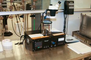
Our Strip annealer is primarily used for ohmic contact formation on III-V compound semiconductors. The system runs in a forming gas environment to keep oxygen contamination minimized. Temperature of the graphite strip is electronically controlled to prevent overshoot and the phase changes of the metal can be observed through the stereo microscope while annealing is taking place. This observation is often the best way to get the best ohmic contact. Thermal interlocks prevent the system from overheating and maximum anneal times are on the order of several minutes. Anneals up to 500°C are permitted. The graphite strip is only 1.5 inches wide, limiting the sample size.
Detailed Specifications
- Temperatures up to 500°C for several minutes
- Forming gas ambient
- Sample size limited to 1.5 inches on a side
- Electronic temperature control
- Maximum sample size ~ 1.5 inches square
- Stereo microscope for viewing the contact phase change
