ICP-Etch (Unaxis VLR): Difference between revisions
| Line 26: | Line 26: | ||
=Documentation= |
=Documentation= |
||
*[[media:UnaxisICPInstructions.pdf|Operating Instructions]] |
*[[media:UnaxisICPInstructions.pdf|Operating Instructions]] |
||
*[[media:InP Etch-200C-ningSheet1.pdf|Standard Recipes]] |
|||
Revision as of 21:45, 8 August 2012
| |||||||||||||||||||||
About
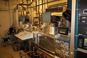
This system is configured as an ICP etching tool with 1000 W ICP power, 500 W RF substrate power, and RT - 200°C operation with back-side He cooling and a clamp to maintain controlled surface temperatures during etching. This chamber has Cl2, BCl3, Ar, N2, and O2 for gas sources and can be used to etch a variety of materials from compound semiconductors to metals. The high temperature etching is specifically useful for etching of high Indium containing compound semiconductors such as InP, where etch product volatility is an issue. High aspect ratio, smooth vertical wall, InP and related compound semiconductor (InGaAs, InAlAs, InGaAsP, etc.) etching is done in this system. The chamber is configured for 4" wafers. Pieces are handled by using a silicone-based thermal heat sink compound. Both sapphire and silicon carrier wafers are available. Laser end-point monitoring is also included in the system.
Detailed Specifications
- 1000 W ICP source, 500 W RF Sample Bias Source in etching chamber
- RT - 200°C sample temperature for etching
- Laser monitoring available
- Cl2, BCl3, Ar, N2, and O2 in etch chamber
- Multiple 4” diameter wafer capable system
- Pieces possible by mounting to 4 ” wafer with thermal compound
