Wafer Bonder (Logitech WBS7): Difference between revisions
Freeborn d (talk | contribs) |
real photo of the tool |
||
| Line 1: | Line 1: | ||
{{tool|{{PAGENAME}} |
{{tool|{{PAGENAME}} |
||
|picture= |
|picture=Logitech_WSBU-6_Wafer_Bonder_-_photo_-_800px.png |
||
|type = Thermal Processing |
|type = Thermal Processing |
||
|super= Don Freeborn |
|super= Don Freeborn |
||
Revision as of 17:08, 9 April 2019
|
About
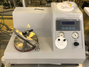
This tool is most often used for bonding samples to Silicon carrier wafers with CrystalBond wax. This can be used for through-etching of the sample wafer, for dicing, or sometimes for lithography.
A user can place the two wafers to be bonded in contact, with the adhesive in between (such as wax, photoresist etc.). A rubber membrane is lowered on top, creating a small vacuum chamber. The tool can then be programmed to heat the wafers and melt the wax/cure the adhesive, while vacuum is pulled in the chamber, which pulls the rubber membrane down onto the top wafer. This flattens the bond and evacuates bubbles from between the wafers, providing a planar bond.
We also have recipes for spin-coating the crystalbond wax, allowing for a uniform coating of the adhesive wax.
Detailed Specifications
- Substrate Size: 4"-6"
- Temperature Range: 20c-188c
Operation Procedures
Recipes
- Recipes > Packaging Recipes > Wafer Bonder (Logitech WBS7)
