PECVD Recipes: Difference between revisions
→SiN deposition (Unaxis VLR): change in name of recipe |
→SiO2 250C Data 2019: recipe cleanup |
||
| Line 105: | Line 105: | ||
==== Standard Recipe ==== |
==== Standard Recipe ==== |
||
*[//wiki.nanotech.ucsb.edu/wiki/images/ |
*[//wiki.nanotech.ucsb.edu/wiki/images/b/b0/STD_SiO2_5-9-18.pdf STD Oxide recipe(update this page)] |
||
| ⚫ | |||
*[//wiki.nanotech.ucsb.edu/wiki/images/b/b0/STD_SiO2_5-9-18.pdf STD SiO2 5/9/18] |
|||
| ⚫ | |||
==== Historical Data ==== |
==== Historical Data ==== |
||
| Line 136: | Line 135: | ||
*[//wiki.nanotech.ucsb.edu/wiki/images/4/4c/SiNx_Films_by_PECVD2.pdf SiNx Film Stress vs LF and HF Duration Time, and Gas Flowing-rate] |
*[//wiki.nanotech.ucsb.edu/wiki/images/4/4c/SiNx_Films_by_PECVD2.pdf SiNx Film Stress vs LF and HF Duration Time, and Gas Flowing-rate] |
||
*[//wiki.nanotech.ucsb.edu/wiki/images/ |
*[//wiki.nanotech.ucsb.edu/wiki/images/5/52/STD_Nitride_5-9-18_Dep.recipe.pdf STD Nitride2 Standard Recipe (update this page)] |
||
| ⚫ | |||
*[//wiki.nanotech.ucsb.edu/wiki/images/5/52/STD_Nitride_5-9-18_Dep.recipe.pdf STD Nitride2 Standard Recipe 5/9/2018] |
|||
| ⚫ | |||
==== Historical Data ==== |
==== Historical Data ==== |
||
| Line 167: | Line 165: | ||
==== Standard Recipe ==== |
==== Standard Recipe ==== |
||
*[//wiki.nanotech.ucsb.edu/wiki/images/9/98/STD_LSNitride2_12-14-18_recipe.pdf STD LSNitride2 |
*[//wiki.nanotech.ucsb.edu/wiki/images/9/98/STD_LSNitride2_12-14-18_recipe.pdf STD LSNitride2 (update this page)] |
||
*[https://docs.google.com/spreadsheets/d/1qXCH1phgvk3-5_5FUqeQaGPERhyS5dn4/edit#gid= |
*[https://docs.google.com/spreadsheets/d/1qXCH1phgvk3-5_5FUqeQaGPERhyS5dn4/edit#gid= STD LS Nitride2 Recipe Parameters] |
||
*''Old Versions:'' |
*''Old Versions:'' |
||
**[//wiki.nanotech.ucsb.edu/wiki/images/a/a5/New_AdvPECVD-LS_Nitride2_300C_standard_recipe_LS_Nitride2_standard_recipe.pdf LS Nitride2 Standard Recipe 2014-5/9/2018] |
**[//wiki.nanotech.ucsb.edu/wiki/images/a/a5/New_AdvPECVD-LS_Nitride2_300C_standard_recipe_LS_Nitride2_standard_recipe.pdf LS Nitride2 Standard Recipe 2014-5/9/2018] |
||
| Line 228: | Line 226: | ||
=== SiO2 250C Data 2019 === |
=== SiO2 250C Data 2019 === |
||
| ⚫ | |||
| ⚫ | |||
*[https://docs.google.com/spreadsheets/d/1wocoCPOOEDQcZbXJJNaZs1sr9dXBZpn1wUyglL8IQrI/edit#gid=sharing SiO2 LDR 250C 300nm Data-2019] |
*[https://docs.google.com/spreadsheets/d/1wocoCPOOEDQcZbXJJNaZs1sr9dXBZpn1wUyglL8IQrI/edit#gid=sharing SiO2 LDR 250C 300nm Data-2019] |
||
*[https://docs.google.com/spreadsheets/d/16s-tUna9xrkKneK1lE-qSPuUHWlDmP6Qu3IngBXP3R8/edit#gid=sharing SiO2 HDR 250C 300nm Data-2019] |
*[https://docs.google.com/spreadsheets/d/16s-tUna9xrkKneK1lE-qSPuUHWlDmP6Qu3IngBXP3R8/edit#gid=sharing SiO2 HDR 250C 300nm Data-2019] |
||
*[https://docs.google.com/spreadsheets/d/1Xi21OrargcNRthZ2fM_56APB8O599ctDfq5E_6B5Ft0/edit#gid=sharing Thickness Uniformity SiO2 LDR 250C 300nm-2019] |
*[https://docs.google.com/spreadsheets/d/1Xi21OrargcNRthZ2fM_56APB8O599ctDfq5E_6B5Ft0/edit#gid=sharing Thickness Uniformity SiO2 LDR 250C 300nm-2019] |
||
*[https://docs.google.com/spreadsheets/d/1Mm_rsTm9xDQ50kZx6X6EZ5dTegUvinq0zFxRtE8B2R4/edit#gid=sharing Thickness Uniformity SiO2 HDR 250C 300nm-2019] |
*[https://docs.google.com/spreadsheets/d/1Mm_rsTm9xDQ50kZx6X6EZ5dTegUvinq0zFxRtE8B2R4/edit#gid=sharing Thickness Uniformity SiO2 HDR 250C 300nm-2019] |
||
| ⚫ | |||
| ⚫ | |||
===SiO2 250C Data 2020=== |
===SiO2 250C Data 2020=== |
||
| ⚫ | |||
| ⚫ | |||
*[https://docs.google.com/spreadsheets/d/1bU2Gu3x3DNyrq8skMAQZJCsra-IcoDCT0U5D135YPgc/edit#gid=sharing SiO2 LDR 250C 300nm Data-2020] |
*[https://docs.google.com/spreadsheets/d/1bU2Gu3x3DNyrq8skMAQZJCsra-IcoDCT0U5D135YPgc/edit#gid=sharing SiO2 LDR 250C 300nm Data-2020] |
||
*[https://docs.google.com/spreadsheets/d/1OxHi5r9ifNvF8ODpIk6aoRevb4RdbbykwPVMm1g-yi4/edit#gid=sharing SiO2 HDR 250C 300nm Data-2020] |
*[https://docs.google.com/spreadsheets/d/1OxHi5r9ifNvF8ODpIk6aoRevb4RdbbykwPVMm1g-yi4/edit#gid=sharing SiO2 HDR 250C 300nm Data-2020] |
||
*[https://docs.google.com/spreadsheets/d/1-ytu5R75FAXNfhJZTRuK2eRZyu_L6Hy1BWV2zN6_tRA/edit#gid=sharing Thickness Uniformity SiO2 LDR 250C 300nm-2020] |
*[https://docs.google.com/spreadsheets/d/1-ytu5R75FAXNfhJZTRuK2eRZyu_L6Hy1BWV2zN6_tRA/edit#gid=sharing Thickness Uniformity SiO2 LDR 250C 300nm-2020] |
||
*[https://docs.google.com/spreadsheets/d/1nzVeCKsmgL17zft6axQlixpvsEowJOG7qCnLQm_0XxE/edit#gid=sharing Thickness Uniformity SiO2 HDR 250C 300nm-2020] |
*[https://docs.google.com/spreadsheets/d/1nzVeCKsmgL17zft6axQlixpvsEowJOG7qCnLQm_0XxE/edit#gid=sharing Thickness Uniformity SiO2 HDR 250C 300nm-2020] |
||
| ⚫ | |||
| ⚫ | |||
== Cleaning Recipes (Unaxis VLR Dep) == |
== Cleaning Recipes (Unaxis VLR Dep) == |
||
Revision as of 21:10, 20 April 2020
Back to Vacuum Deposition Recipes.
PECVD 1 (PlasmaTherm 790)
Historical Particulate Data
- Particulates(Gain4) in PECVD#1-OLD DATA 2015
- Particulates(Gain4) in PECVD#1-OLD DATA 2016
- Particulates(Gain4) in PECVD#1-OLD DATA 2017
- Particulates in PECVD#1 films 2017
- Particulates in PECVD#1 films 2018
- Particulates in PECVD#1 films 2019
- Particulates in PECVD#1 films 2020
SiN deposition (PECVD #1)
Historical Data
Thin-Film Properties
- SiN 100nm Data 2014
- SiN 100nm Data 2015
- SiN 100nm Data 2016
- SiN 100nm Data 2017
- SiN 300nm Data 2017
- SiN 300nm Data 2018
- SiN 300nm Data 2019
- SiN 300nm Data 2020
Uniformity Data
- SiN 100 nm Thickness uniformity 2014
- SiN 100 nm Thickness uniformity 2015
- SiN 100 nm Thickness uniformity 2016
- SiN 100 nm Thickness uniformity 2017
- SiN 300nm Thickness uniformity 2017
- SiN 300nm Thickness uniformity 2018
- SiN 300nm Thickness uniformity 2019
- SiN 300nm Thickness uniformity 2020
SiO2 deposition (PECVD #1)
Historical Data
Thin-Film Properties
- SiO2 100nm Data 2014
- SiO2 100nm Data 2015
- SiO2 100nm Data 2016
- SiO2 100nm Data 2017
- SiO2 300nm Data 2017
- SiO2 300nm Data 2018
- SiO2 300nm Data 2019
- SiO2 300nm Data 2020
Uniformity Data
- SiO2 100nm Thickness uniformity 2014
- SiO2 100 nm Thickness uniformity 2015
- SiO2 100 nmThickness uniformity 2016
- SiO2 100nm Thickness uniformity 2017
- SiO2 300nm Thickness uniformity 2017
- SiO2 300nm Thickness uniformity 2018
- SiO2 300nm Thickness uniformity 2019
- SiO2 300nm Thickness uniformity 2020
Low-Stress SiN - LS-SiN (PECVD#1)
SiOxNy deposition (PECVD #1)
Cleaning Recipes (PECVD #1)
The cleaning procedure is very important in order to have consistent result on this tool and also to keep particulate count low. After each deposition you should clean the tool following instructions carefully. The clean is done in two steps:
- Wet cleaning (start cleaning by using a cleanroom wipe sprayed with DI. Wipe chamber sidewalls with it. Finish cleaning by using the cleanroom wipe sprayed with IPA. )
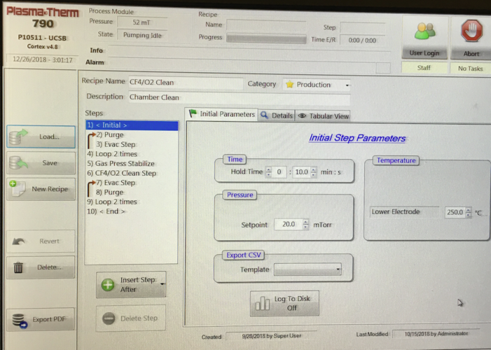
- Load the recipe for cleaning " CF4/O2 Clean" (edit the recipe and change ONLY time of cleaning). Follow instructions regarding a required time for cleaning.
" CF4/O2 Clean recipe"

PECVD 2 (Advanced Vacuum)
Historical Particulate Data
- Particulates (Gain4) in PECVD#2 2015
- Particulates (Gain4) in PECVD#2 2016
- Particulates (Gain4) in PECVD#2 2017
- Particulates in PECVD#2 films 2017
- Particulates in PECVD#2 films 2018
- Particulates in PECVD#2 films 2019
- Particulates in PECVD#2 films 2020
SiO2 deposition (PECVD #2)
Standard Recipe
Historical Data
Thin-Film Properties
- Oxide Data 2014
- Oxide Data 2015
- Oxide data 2016
- Oxide Data 2017
- Oxide Data 2018
- Oxide Data 2019
- Oxide Data 2020
Uniformity Data
- Oxide Thickness Uniformity 2014
- Oxide Thickness Uniformity 2015
- Oxide Thickness Uniformity 2016
- Oxide Thickness Uniformity 2017
- Oxide Thickness Uniformity 2018
- Oxide Thickness Uniformity 2019
- Oxide Thickness Uniformity 2020
SiN deposition (PECVD #2)
Standard Recipe
- SiNx Film Stress vs LF and HF Duration Time, and Gas Flowing-rate
- STD Nitride2 Standard Recipe (update this page)
- STD Nitride2 Recipe Parameters
Historical Data
Thin-Film Properties
- Nitride2 Data 2014
- Nitride2 Data 2015
- Nitride2 Data 2016
- Nitride2 Data 2017
- Nitride2 Data 2018
- Nitride2 Data 2019
- Nitride2 Data 2020
Uniformity Data
- Nitride2 Thickness Uniformity 2014
- Nitride2 Thickness Uniformity 2015
- Nitride2 Thickness Uniformity 2016
- Nitride2 Thickness Uniformity 2017
- Nitride2 Thickness Uniformity 2018
- Nitride2 Thickness Uniformity 2019
- Nitride2 Thickness Uniformity 2020
Low-Stress SiN deposition (PECVD #2)
Low-Stress SilIcon Nitride (< 100 MPa)
Standard Recipe
Historical Data
Thin-Film Properties
- LS Nitride2 Data 2014
- LS Nitride2 Data 2015
- LS Nitride2 Data 2016
- LS Nitride2 Data 2017
- LS Nitride2 Data 2018
- LS Nitride2 Data 2019
- LS Nitride2 Data 2020
Uniformity Data
- LS Nitride2 Thickness Uniformity 2014
- LS Nitride2 Thickness Uniformity 2015
- LS Nitride2 Thickness Uniformity 2016
- LS Nitride2 Thickness Uniformity 2017
- LS Nitride2 Thickness Uniformity 2018
- LS Nitride2 Thickness Uniformity 2019
- LS Nitride2 Thickness Uniformity 2020
Amorphous-Si deposition (PECVD #2)
Cleaning Recipes (PECVD #2)
The cleaning procedure is very important in order to have consistent result on this tool and also to keep particulate count low. After each deposition you should clean the tool following instructions carefully. The clean is done in two steps:
- Wet cleaning (start cleaning by using a cleanroom wipe sprayed with DI. Wipe chamber sidewalls with it. Finish cleaning by using the cleanroom wipe sprayed with IPA. )
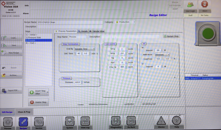
- Load the recipe for cleaning " STD CF4/O2 Clean" (edit the recipe and change ONLY time of cleaning). Follow instructions regarding a required time for cleaning.
" STD CF4/O2 Clean recipe"

ICP-PECVD (Unaxis VLR)
Historical Particulate Data
SiN deposition (Unaxis VLR)
SiN 250C Data 2020
SiN LS 250C Data 2020
- SiN LS 250C 300nm Data-2020
- Thickness Uniformity SiN LS 250C 300nm-2020
- SiN LS 250C Recipe Parameters-2020
SiO2 deposition (Unaxis VLR)
SiO2 250C Data 2019
- SiO2 LDR 250C 300nm Data-2019
- SiO2 HDR 250C 300nm Data-2019
- Thickness Uniformity SiO2 LDR 250C 300nm-2019
- Thickness Uniformity SiO2 HDR 250C 300nm-2019
- SiO2 LDR 250C Recipe Parameters-2019
- SiO2 HDR 250C Recipe Parameters-2019
SiO2 250C Data 2020
- SiO2 LDR 250C 300nm Data-2020
- SiO2 HDR 250C 300nm Data-2020
- Thickness Uniformity SiO2 LDR 250C 300nm-2020
- Thickness Uniformity SiO2 HDR 250C 300nm-2020
- SiO2 LDR 250C Recipe Parameters-2020
- SiO2 HDR 250C Recipe Parameters-2020
Cleaning Recipes (Unaxis VLR Dep)
You must edit the Post-Dep Clean recipe to correspond to your deposited thickness and material. See the Operating Procedure on the Unaxis Tool Page for details.
- SiNx etches at 20nm/min
- SiO2 etches at 40nm/min
" Post-Dep Clean" recipe
Add the picture of " Post-Dep Clean" recipe