ICP-PECVD (Unaxis VLR): Difference between revisions
Jump to navigation
Jump to search
Content deleted Content added
| Line 21: | Line 21: | ||
*Multiple 4” diameter wafer capable system |
*Multiple 4” diameter wafer capable system |
||
*Pieces possible by mounting or placing on 4 ” wafer |
*Pieces possible by mounting or placing on 4 ” wafer |
||
=Documentation= |
|||
*[[media:Operating Instructions (Unaxis VLR).pdf|Operating Instructions]] |
|||
*[[Standard recipes for deposition]] |
|||
Revision as of 15:11, 17 August 2012
| |||||||||||||||||||||
About
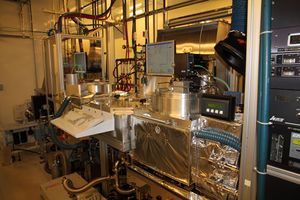
This system is configured as an ICP PECVD deposition tool with 1000 W ICP power, 600 W RF substrate power, and RT-350°C operation. This chamber has 100% SiH4, N2, O2, and Ar for gas sources. The high density PECVD produces a more dense, higher quality SiO2 and Si3N4, as compared with conventional PECVD. With the high density plasma, deposition of high quality films can be done down to below 50°C for processes requiring lower temperatures. Stress compensation for silicon nitride is characterized.
Detailed Specifications
- 1000W ICP source, 600W RF Sample Bias Source in etching chamber
- RT - 350°C sample temperature
- 100% SiH4, Ar, N2, O2
- Multiple 4” diameter wafer capable system
- Pieces possible by mounting or placing on 4 ” wafer
