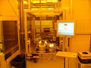
Plasma Activation (EVG 810)
| ||||||||||||||||||||||||||||||
About
This a capacitively coupled Oxygen plasma activation system used exclusively for the surface activation of clean surfaces prior to wafer bonding. This technique allows bonding temperatures to be lowered and is used as a companion tool to the Karl-Suss SB6 wafer bond tool.
No etching nor photoresist is allowed in this tool!
It is for "clean" bonding activation only, not plasma etching.
Detailed Specifications
- Gases used: O2 and N2
- Sample size: pieces to 6” wafer
- Recipes characterized for substrate thicknesses between 250um and 750um. Thicknesses outside of this range need to have parameters optimized to minimize reflective power.
Documentation
Recipes
Please see the Oxygen Plasma Recipe page for standard EVG recipes.
Examples
"Spontaneous" SiO2-SiO2 bonding between a fused-silica SiO2 wafer and Thermally-oxidize Silicon wafer:

Note the pre-bonding wafer-cleaning process is critical. Each "rainbow" in the above indicates a "particle" trapped between the wafer surfaces, particle thickness corresponds to lateral debonded radius. This example was aligned by hand after EVG O2 activation, no anneal performed afterward. Processing developed, performed and photographed by Demis D. John.
