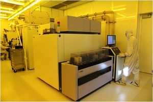
Stepper 3 (ASML DUV)
|
About
The ASML 5500 stepper is a 248nm DUV stepper for imaging dense features down to below 200nm and isolated line structures down to below 150nm. Overlay accuracy is better than 30nm. The system is configured for 4” wafers and, with staff support, mounted pieces down to 14mm in size can be exposed using a 4” wafer as a carrier. The system is designed for high throughput, so shooting multiple 4" wafers is extremely fast. Additionally, the litho programming is highly programmable, allowing for very flexible exposures of multiple aligned patterns from multiple masks in a single session, allowing for process optimization of large vs. small features in a single lithography.
The full field useable exposure area is limited to the intersection of a 31mm diameter circle and a rectangle of dimensions 22mm x 27mm. The system has a variable NA system and has a square field image size of 21 x 21mm for 0.63 NA and a square field image size of 22mm x 22mm for 0.4 to 0.57 NA.
Other rectangular sizes available: 21mm x 23mm; 20mm x 24mm; 19mm x 25mm; 18mm x 25.5mm; 17mm x 26mm; 16mm x 26.5mm; 15mm x 27mm.
Resists Used (see PhotoLith Recipes for processing info):
- UV210-0.3 - Positive: 300nm nominal thickness
- UV6-0.8 - Positive: 800nm nominal thickness
- UV26-2.5 - Positive: 2.5um nominal thickness
- UVN2300-0.5 - Negative: 500nm nominal thickness
- AR2/DUV42P-6/DS-K101: Anti-Reflective Coatings
- PMGI: Underlayer
AZ300MIF Developer for all processes
