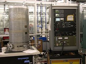
E-Beam 2 (Custom)
| |||||||||||||||||||||
About
This electron-beam evaporation system is used for the controlled deposition of thin dielectric films. The films are evaporated from a wide variety of solid sources. The most common dielectrics deposited are: SiO2, SiO, TiO2, Ta2O5, SrF2. Other materials may be evaporated upon request. Oxygen gas can be bled into the system during deposition to try to maintain the stoichiometry during deposition. Fixturing for heating the substrate can also be used. A crystal thickness monitor is used to control the deposition thickness. The dielectrics deposited by this system are typically used for optical coatings (anti-reflective and highly reflective multiple layer stacks), electrical insulators, and reactive ion etching masks. Samples up to ~ 3” x 3” can be placed into this system for evaporation. Typical deposition rates are several Angstroms/second.
Detailed Specifications
- Temescal 10kV power supply
- Temescal 4-pocket series 260 e-beam source
- Electron beam controller with sweep rate and amplitude control
- Cryo-pumped system with ~ 1e-7 ultimate base pressure
- Automatic vacuum sequencing
- Crystal thickness monitoring
- Sample size: up to 3” x 3” pieces
- Oxygen bleed for maintaining oxide stoichiometry
Materials Table
Materials Table
| ||||
|---|---|---|---|---|
| Material | Density, g/cm3 | Z Ratio | Tooling factor, % | Comments |
| Al2O3 | 3.97 | 0.336 | 140.0 | Tony could you please check this? |
| GeO2 | 6.24 | 1.000 | 139.0 | |
| ITO | 7.16 | 1.000 | 139.0 | Density should be 6.43-7.14, z ratio? |
| MgO | 3.58 | 0.411 | 157.6 | OK |
| Si | 2.32 | 0.712 | 150.0 | |
| SiO2 | 2.20 | 1.070 | 157.6 | Should be 2.648, z ratio 1.000 |
| SiOx | 2.13 | 0.87 | 130.0 | |
| SrF2 | 4.28 | 0.727 | 140.0 | |
| Ta2O5 | 8.2 | 0.30 | 157.6 | |
| TiO2 | 4.26 | 0.400 | 139.0 | |
