Packaging Recipes: Difference between revisions
(→Dicing Saw Recipes (ADT 7100): added Dicing Tips) |
(→Calculated Blade Exposures: added blade exposure calc) |
||
| Line 83: | Line 83: | ||
|} |
|} |
||
==== |
====Anatomy of a Blade==== |
||
Example: '''2.187-4C-9RU-3''' |
Example: '''2.187-4C-9RU-3''' |
||
| Line 124: | Line 124: | ||
| |
| |
||
|} |
|} |
||
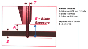
==== Blade Exposure Calculation ==== |
|||
[[File:ADT Dicing - Blade Exposure diagram.png|alt=schematic of blade exposure|none|thumb|386.5874938964844x386.5874938964844px|Diagram of blade exposure]] |
|||
===Mounting/Unmounting Samples=== |
===Mounting/Unmounting Samples=== |
||
The UV-Release Tape dispenser is most-often used for mounting sample for dicing. |
The UV-Release Tape dispenser is most-often used for mounting sample for dicing. |
||
| Line 133: | Line 137: | ||
*Partial Release for Shipping: 9 sec exposure |
*Partial Release for Shipping: 9 sec exposure |
||
=== |
===Dicing Tips=== |
||
Harder materials will often require larger diamond particle sizes, and thicker blades will last longer if they are overheating and breaking often. |
Harder materials will often require larger diamond particle sizes, and thicker blades will last longer if they are overheating and breaking often. |
||
Revision as of 19:51, 4 January 2022
Dicing Saw Recipes (ADT 7100)
Recommended Dicing Parameters
This table is for our stocked Thermocarbon Resnoid blades.
-4C blades are 4mils/100µm wide, while -8C blades are 8mils/200µm wide. Plan for ~50–100µm extra edge clearance to account for chipping etc.
Narrower (~30-50µm) Nickel Hubbed blades are often used for even narrower dicing streets, these must be purchased by the user.
| Material | Blade P/N | Spindle Speed
(KRPM) |
Cut Speed
(mm/s) |
|---|---|---|---|
| Alumina, AlN | 2.187-8C-54RU-3 | 25 | 0.5-2 |
| Ceramic | 2.187-4C-30RU-3 | 18 | 0.5-2 |
| GaAs | 2.187-4C-9RU-3 | 35 | 1-5 |
| GaN (<550um) | 2.187-4C-30RU-3 | 35 | 0.5-3 |
| GaN (>550um) | 2.187-8C-30RU-3 | 35 | 0.5-2 |
| Glass/Fused Silica | 2.187-4C-22RU-3 | 25 | 1-5 |
| InP | 2.187-4C-9RU-3 | 35 | 1-5 |
| Quartz | 2.187-4C-30RU-3 | 25 | 1-5 |
| Sapphire | 2.187-8C-54RU-3 | 18 | 0.5-2 |
| Si | 2.187-4C-9RU-3 | 35 | 4-10 |
| Si on Glasss | 2.187-4C-9RU-3 | 25 | 1-5 |
| SiC | 2.187-8C-30RU-3 | 25 | 0.5-2 |
| Ti | 2.187-8C-54RU-3 | 15 | 0.5-2 |
Anatomy of a Blade
Example: 2.187-4C-9RU-3
"2.187": This is the blade Diameter in inches (55.56mm).
"4C": Blade thickness in mils. 4mil = 100µm
"9RU": Diamond particle size in microns. Stocked resin blades have embedded diamond particles. Smaller particles create a smoother kerf, but remove less material and are thus less robust (or require slower cutting speeds) "RU-3" is a blade parameter that deals with cut quality vs. robustness (lifetime) of the blade.
Calculated Blade Exposures
| Blade Diam | Flange Diam. | Blade Exposure | |
|---|---|---|---|
| 2.187" (55.55mm) | 47mm | 4.275mm | |
| 2.187" (55.55mm) | 49mm | 3.275mm | |
| 2.187" (55.55mm) | 51mm | 2.275mm | 51mm Currently Unavailable |
| 2.187" (55.55mm) | 52mm | 1.775mm | |
| 2.187" (55.55mm) | 53mm | 1.275mm |
Blade Exposure Calculation
Mounting/Unmounting Samples
The UV-Release Tape dispenser is most-often used for mounting sample for dicing.
The Tape Model installed is Ultron 1042R. Data Sheet Here.
- Procedure for mounting sample on UV-Release Tape
- Full Release: 60 sec exposure
- Partial Release for Shipping: 9 sec exposure
Dicing Tips
Harder materials will often require larger diamond particle sizes, and thicker blades will last longer if they are overheating and breaking often.
It is not uncommon to have to change a blade in the middle of cutting a wafer - the software is set up to allow this easily without aborting the programmed cuts. The "Height Check Rate" in the recipe will check the blade exposure after this many cuts, using the optical height sensor - this allows you to see how quickly the blade is wearing out (as blade exposure reduces).
Ensuring the cut water jet is hitting at ~7-8 o'clock on the blade and the water jet is being split in two will keep the blade coolest and help prevent breakage. Water sprays should be set to 0.9/0.9/0.9 by default.
For sapphire dicing (very hard material), it is common to use "double-pass dicing", where the substrate is cut at only half depth (eg. cutting only 150µm deep for a 300µm thick substrate) on the first pass, and then re-cut at the full depth. The blade will need to be changed often, so set your "Height Check Rate" to 1 or 2. This can be very time consuming. 200-300µm thick Sapphire substrates are much easier to cut than 650µm thick - often single-pass dicing is adequate for the thinner substrates.
Surface Protection
Photoresist
Users most often use sacrificial photoresists to protect the surface from accumulating dicing dust. The static-buildup of dielectric films causes the dust to adhere strongly. Ensure that the PR thickness will adequately coat all your exposed topography (eg. use a ≥2µm thick PR for protecting 1.5-2.0µm tall etched features).
- Choose a photoresist of appropriate thickness, and spin-coat it & soft-bake it according to a standard recipe.
- Perform your dicing
- Remove the die from the UV release tape (60sec UV Exposure)
- Strip the PR from each die in Acetone and ISO & N2 dry
Blue Tape
Alternatively our low-tack residue-free Blue tape can be used to protect the die surface. Blue tape removal is easy for large die, but does require manual removal from each die, and eliminates sample exposure to solvents.
The very edges of the die may accumulate a bit more dicing dust due to the tape delaminating slightly during dicing. Plan for about 50-100µm of edge clearance on each die.
Wafer Bonder (Logitech WBS7)
This tool is used for bonding samples to Silicon carrier wafers with CrystalBond wax.
