Ion Beam Deposition (Veeco NEXUS): Difference between revisions
(added schematic of ion beam) |
|||
| Line 46: | Line 46: | ||
*[[Sputtering_Recipes#Ion_Beam_Deposition_.28Veeco_NEXUS.29|Sputtering Recipes: Ion Beam Deposition (Veeco NEXUS)]] |
*[[Sputtering_Recipes#Ion_Beam_Deposition_.28Veeco_NEXUS.29|Sputtering Recipes: Ion Beam Deposition (Veeco NEXUS)]] |
||
**''Dep Rates, Refractive Indices etc. for various available dielectric coatings'' |
**''Dep Rates, Refractive Indices etc. for various available dielectric coatings'' |
||
*[[IBD: Calibrating Optical Thickness|Method for accurately calibrating optical films]]: For example, for calibrating and depositing Multi-layer DBR gratings, Anti-Reflection coatings etc. |
*[[IBD: Calibrating Optical Thickness|Method for accurately calibrating multi-layer optical films]]: For example, for calibrating and depositing Multi-layer DBR gratings, Anti-Reflection coatings etc. |
||
== |
==Schematics/Examples== |
||
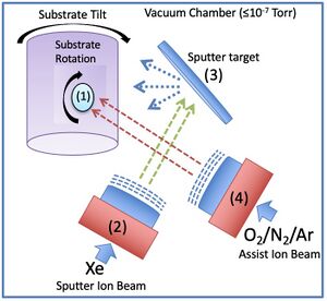
[[File:IBD Schematic.jpg|alt=Illustration showing wafer, assist beam and sputter/depo beam|none|thumb|Top-Down Schematic of the Ion Beam Deposition system, where (1) is the substrate/wafer, (2) is the Depo/Sputter ion beam, (3) is the variable sputter target (either Si, Ta, Al, or Ti), and (4) is the Assist Ion Beam.]] |
[[File:IBD Schematic.jpg|alt=Illustration showing wafer, assist beam and sputter/depo beam|none|thumb|Top-Down Schematic of the Ion Beam Deposition system, where (1) is the substrate/wafer, (2) is the Depo/Sputter ion beam, (3) is the variable sputter target (either Si, Ta, Al, or Ti), and (4) is the Assist Ion Beam.]] |
||
<br /> |
<br /> |
||
Revision as of 04:33, 22 September 2023
| ||||||||||||||||||||||||||||||
About
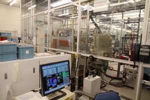
This tool is designed for high quality, precise, reproducible deposition of dielectric films for optical quality films. Metallic material is ion bombarded from a target material and a reactive ion beam of oxygen and/or nitrogen is aimed at the surface, creating a metal-oxide or nitride on the sample. The system is fully computer controlled to facilitate multi-layer stack recipes for high reflectivity or low reflectivity coatings. The system is load locked and can handle wafers up to 6” in diameter as well as small pieces. Sample rotation and angling is used to facilitate material quality and allows for sidewall coverage on non-planar surfaces. Uniformity is better than 1.5% over 6" wafers and reproducibility is expected to be within one percent (with pre-dep calibration). The high-energy sputter deposition produces denser films than other techniques, improving optical damage threshold (and thus coating lifetime). This also causes the refractive indices to be slightly higher than comparable stoichiometric films deposited by other techniques.
Four metallic targets can be installed (producing Oxides & Nitrides of each). Ta & Si are always available, the others are rotated out as users need them.
The most common films for High-/Anti-Reflection (HR/AR) coatings are SiO2 & Ta2O5, both of which are extremely stable w/r/to refractive index. Users typically calibrate their dep. rates prior to critical deps. & multi-layer coatings.
Detailed Specifications
- Full programmable control through GUI, designed for multi-layer optical coatings
- Xenon sputter-target bombardment
- Nitrogen and/or Oxygen deposition assist source for metal oxides/nitrides
- Available Sputter Targets: Ta, Si, Al, Ti (ITO target on-hand but not installed)
- Standard Recipes: Ta2O5, SiO2, Si3N4, TiO2, Al2O3.
- Custom recipes: SiOxNy, AlN, TaN, TiN
- Argon sample cleaning/pre-sputtering with low energy/etch rate
- Base Pressure ≤ 3e-8 Torr
- Accepts small pieces, up to 6” wafers accepted
- Holders available for etched/cleaved facet coating
- High quality, High Reflectivity DBR (>99.5%) mirrors demonstrated at UV-Vis & near-IR wavelengths
- Wide-band Anti-Reflection coatings demonstrated in near-IR (~1550nm)
Documentation
Recipes
- Sputtering Recipes: Ion Beam Deposition (Veeco NEXUS)
- Dep Rates, Refractive Indices etc. for various available dielectric coatings
- Method for accurately calibrating multi-layer optical films: For example, for calibrating and depositing Multi-layer DBR gratings, Anti-Reflection coatings etc.
Schematics/Examples

