Stepper 1 (GCA 6300): Difference between revisions
| Line 45: | Line 45: | ||
=Operating Procedures= |
=Operating Procedures= |
||
| ⚫ | |||
* [https://wiki.nanofab.ucsb.edu/w/images/b/bb/GCA_6300_Standard_Operating_Procedure_122823.pdf SOP] * |
* [https://wiki.nanofab.ucsb.edu/w/images/b/bb/GCA_6300_Standard_Operating_Procedure_122823.pdf SOP] * |
||
* [https://wiki.nanofab.ucsb.edu/w/images/a/a0/GCA_6300_Running_a_JOB_3.pdf Running the JOB] * |
* [https://wiki.nanofab.ucsb.edu/w/images/a/a0/GCA_6300_Running_a_JOB_3.pdf Running the JOB] * |
||
* [https://wiki.nanofab.ucsb.edu/w/images/9/93/GCA6300_Optimizing_the_process_6.pdf Optimizing the Process] * |
* [https://wiki.nanofab.ucsb.edu/w/images/9/93/GCA6300_Optimizing_the_process_6.pdf Optimizing the Process] * |
||
* [https://wiki.nanofab.ucsb.edu/w/images/3/32/GCA_6300_Programming_a_Job_7.pdf Programming a Job] * |
* [https://wiki.nanofab.ucsb.edu/w/images/3/32/GCA_6300_Programming_a_Job_7.pdf Programming a Job] * |
||
| ⚫ | |||
*[[Programming a Job]] |
*[[Programming a Job]] |
||
*[[GCA 6300 USer Accessible Commands|GCA 6300 User Accessible Commands]] |
*[[GCA 6300 USer Accessible Commands|GCA 6300 User Accessible Commands]] |
||
Revision as of 19:49, 29 December 2023
| ||||||||||||||||||||||||||||||
About
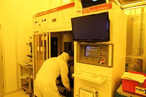
Our GCA wafer stepper is an i-line (365 nm) step and repeat exposure tool for doing lithography that requires high resolution and/or critical alignment. The system has been modified to accept piece parts (down to ~15 mm x 15 mm) up to 6” diameter wafers using manual wafer loading. The maximum square die size is 14.8mm x 14.8mm. The system has an Olympus 2142 (N.A. = 0.42) lens that reduces the mask image by 5 x and gives an ultimate resolution of ~ 0.5 um in the center of the lens field. The system can easily produce 0.7 um isolated lines across the entire field. Autofocus is used to determine the sample surface relative to the lens, making the focus stable and repeatable for different thickness of wafer. The stages are controlled by stepper motors and laser interferometers. Using the global, manual alignment, better than 0.25 um alignment error is achievable. Using the DFAS local alignment system, alignment error better than 0.15 um is achieved. With the 350 W Hg arc lamp, we get approximately 180 mW/cm² of i-line intensity at the wafer.
The system is computer controlled with the capability to program and save a wide variety of exposure jobs. We also have unlimited phone support for system problems through a service contract. The laboratory contains a variety of i-line compatible photoresists. SPR955CM-0.9 for 0.7-1.0 um thick positive processes. AZ5214E for 1.0-2.0 um thick image reversal (negative) process. SPR955CM-1.8 for 1.5-2.0 um thick positive processes. SPR220-3 for 2.5-5 um thick positive process. SPR220-7 for > 5 um thick positive processes. AZnLOF5510 for 1.0um and AZnLOF 2020 for 1.5-3 um negative resist process. Shipley LOL-2000 is also used as an underlayer for high resolution lift-off processes.
Detailed Specifications
- Lens: Olympus 2142: NA = 0.42; Depth of field = 1.2 um for 0.7 um process
- Maximum die size: ~15 mm x 15 mm
- Resolution: 500 nm over portion of field; 700 nm over entire field
- Registration tolerance: Max 0.30 um global alignment; Max 0.15 um local alignment (with care, you can achieve < 0.10 um registration)
- Minimum substrate size: ~ 10 x 10 mm
- Computer programmable recipes saved on hard disk
Process Information
- Process Page: Photolithography Recipes
- GCA 6300 Mask Making Guidance (Work in progress- not ready yet)
CAD Files
- Photomask Template: Dark-field (polygons/objects are clear) at 5x Magnification (GDS)
- This template is designed to be submitted to the photomask vendor to print as-is, no scaling applied.
- Insert your designs into the template as Instances scaled UP by 5x.
- During exposure, set the blades to 90/90 to block out AutoStep200 DFAS openings
- Global Alignment Mark CAD File (GDS)
- See the Calculators + Utilities > CAD Files & Templates page for other useful CAD files, such as overlay verniers, vented fonts etc.
Service Provider
- 3C Technical - The company that services the stepper.
Operating Procedures
- Standard Operating Procedure
- Programming a Job
- GCA 6300 User Accessible Commands
- Troubleshooting and Recovery
Staff Procedures
These procedures are for Staff use - contact staff if you think you need to run these!
