ICP-Etch (Unaxis VLR): Difference between revisions
pasted recipes section |
|||
| (22 intermediate revisions by 6 users not shown) | |||
| Line 1: | Line 1: | ||
{{ |
{{tool2|{{PAGENAME}} |
||
|picture=UnaxisPECVD.jpg |
|picture=UnaxisPECVD.jpg |
||
|type = Dry Etch |
|type = Dry Etch |
||
|super= Tony Bosch |
|super= Tony Bosch |
||
|super2= Don Freeborn |
|||
|phone=(805)839-3918x217 |
|phone=(805)839-3918x217 |
||
|location=Bay 1 |
|location=Bay 1 |
||
| Line 10: | Line 11: | ||
|materials = |
|materials = |
||
|toolid=30 |
|toolid=30 |
||
}} |
}} |
||
'''This tool has been decommissioned. Please use the [[Oxford ICP Etcher (PlasmaPro 100 Cobra)|<u>Oxford Cobra ICP Etcher</u>]] for III-V etching instead. -- 2023 Demis D. John.''' |
|||
| ⚫ | |||
| ⚫ | |||
| ⚫ | This system is configured as an ICP etching tool with 1000 W ICP power, |
||
| ⚫ | This system is configured as an ICP etching tool with 1000 W ICP power, 600 W RF substrate power, and 30C - 200°C operation with back-side He to maintain controlled surface temperatures during etching. This chamber has Cl<sub>2</sub>, BCl<sub>3</sub>, Ar, N<sub>2</sub>, and O<sub>2</sub> for gas sources and can be used to etch a variety of materials from compound semiconductors to metals. The high temperature etching is specifically useful for etching of high Indium containing compound semiconductors such as InP, where etch product volatility is an issue. High aspect ratio, smooth vertical wall, InP and related compound semiconductor (InGaAs, InAlAs, InGaAsP, etc.) etching is done in this system. The chamber is configured for 4" wafers. Pieces are handled by using a silicone-based thermal heat sink compound. Both sapphire and silicon carrier wafers are available. Laser end-point monitoring is also included in the system. |
||
| ⚫ | |||
===Cluster Configuration=== |
|||
| ⚫ | |||
A Deposition and Etch chamber are both attached to the same loadlock, allowing etching and deposition without breaking vacuum. Each chamber can be scheduled separately on SignupMonkey. |
|||
| ⚫ | |||
| ⚫ | |||
*'''PM3''': [[ICP-PECVD (Unaxis VLR)|ICP-PECVD Deposition]] |
|||
| ⚫ | |||
*'''PM1''': ICP Etch (this page) |
|||
| ⚫ | |||
| ⚫ | |||
| ⚫ | |||
| ⚫ | |||
| ⚫ | |||
| ⚫ | |||
| ⚫ | |||
*Pieces possible by mounting to 4 ” wafer with thermal compound |
*Pieces possible by mounting to 4 ” wafer with thermal compound |
||
=Documentation= |
==Documentation== |
||
*[[media:UnaxisICPInstructions.pdf|Operating Instructions]] |
|||
*[//wiki.nanotech.ucsb.edu/wiki/images/8/80/PM1_Wiki_Operational_Procedure_3-14-14.pdf Operating Instructions] |
|||
*[[media:InP Etch-200C-ningSheet1.pdf|Standard Recipes]] |
|||
=Recipes= |
|||
==Process Control Data (Unaxis VLR)== |
|||
*[[Unaxis VLR Etch - Process Control Data|InP Etch - Process Control Data]] |
|||
==GaAs-AlGaAs Etch (Unaxis VLR)== |
|||
*[//wiki.nanotech.ucsb.edu/wiki/images/4/4e/15-GaAs_etch-Unaxis_ICP_etcher.pdf GaAs Etch Recipe (Cl<sub>2</sub>N<sub>2</sub> 30C)] |
|||
*[//wiki.nanotech.ucsb.edu/wiki/images/1/1f/14-AlAs-GR-cal_etch-Unaxis_ICP_etcher.pdf AlGaAs Etch Recipe (Cl<sub>2</sub>N<sub>2</sub> 30C)] |
|||
==InP-InGaAs-InAlAs Etch (Unaxis VLR)== |
|||
*[//wiki.nanotech.ucsb.edu/wiki/images/9/90/18-InP-based_etching-Cl2N2Ar.pdf InP-based Material Etch Profile (Cl<sub>2</sub>N<sub>2</sub>Ar200C)] |
|||
*[//wiki.nanotech.ucsb.edu/wiki/images/a/ad/17-InP%26InGaAs_etch-Cl2H2Ar-Unaxis-VLR.pdf InP-InGaAs Etch Profile (Cl<sub>2</sub>H<sub>2</sub>Ar 200C)] |
|||
*[//wiki.nanotech.ucsb.edu/wiki/images/6/6e/SiO2-Mask_Etch_Recipe_for_Unaxis_Cl2_Etch.pdf Recipe of Etching SiO<sub>2</sub> Mask for Cl<sub>2</sub> Etch (ICP#2)] |
|||
*[[InP Etch Test Result in Details|InP Etch Historical Data (Cl<sub>2</sub>H<sub>2</sub>Ar 200C)]] |
|||
*[[InP Etch Rate and Selectivity (InP/SiO2)|InP Etch Test]] |
|||
*[//wiki.nanotech.ucsb.edu/wiki/images/a/ac/Lower-Etch-Rate_InP_Etch_using_Unaxis_PM1_tool_at_200_C.pdf Lower etch-rate InP Etch (Cl<sub>2</sub>N<sub>2</sub> 200C)] |
|||
==GaN Etch (Unaxis VLR)== |
|||
*[//wiki.nanotech.ucsb.edu/wiki/images/d/df/09-Plasma_Etching_of_GaN-UnaxisPM1.pdf GaN Etch Recipe (Cl<sub>2</sub>BCl<sub>3</sub>N<sub>2</sub>Ar 85C)] |
|||
==GaSb Etch (Unaxis VLR)== |
|||
''Available - ask staff'' |
|||
==Cleaning Recipes (Unaxis VLR)== |
|||
''To Be Added: Required cleaning time & recipes'' |
|||
Latest revision as of 22:38, 6 August 2024
| ||||||||||||||||||||||||||||||
This tool has been decommissioned. Please use the Oxford Cobra ICP Etcher for III-V etching instead. -- 2023 Demis D. John.
About
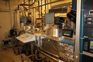
This system is configured as an ICP etching tool with 1000 W ICP power, 600 W RF substrate power, and 30C - 200°C operation with back-side He to maintain controlled surface temperatures during etching. This chamber has Cl2, BCl3, Ar, N2, and O2 for gas sources and can be used to etch a variety of materials from compound semiconductors to metals. The high temperature etching is specifically useful for etching of high Indium containing compound semiconductors such as InP, where etch product volatility is an issue. High aspect ratio, smooth vertical wall, InP and related compound semiconductor (InGaAs, InAlAs, InGaAsP, etc.) etching is done in this system. The chamber is configured for 4" wafers. Pieces are handled by using a silicone-based thermal heat sink compound. Both sapphire and silicon carrier wafers are available. Laser end-point monitoring is also included in the system.
Cluster Configuration
A Deposition and Etch chamber are both attached to the same loadlock, allowing etching and deposition without breaking vacuum. Each chamber can be scheduled separately on SignupMonkey.
- PM3: ICP-PECVD Deposition
- PM1: ICP Etch (this page)
Detailed Specifications
- 1000 W ICP source, 600 W RF Bias Source
- 30 - 200°C sample temperature for etching
- Laser monitoring available
- Cl2, BCl3, Ar, N2, H2, SF6,and O2 in etch chamber
- Multiple 4” diameter wafer capable system
- Pieces possible by mounting to 4 ” wafer with thermal compound
Documentation
Recipes
Process Control Data (Unaxis VLR)
GaAs-AlGaAs Etch (Unaxis VLR)
InP-InGaAs-InAlAs Etch (Unaxis VLR)
- InP-based Material Etch Profile (Cl2N2Ar200C)
- InP-InGaAs Etch Profile (Cl2H2Ar 200C)
- Recipe of Etching SiO2 Mask for Cl2 Etch (ICP#2)
- InP Etch Historical Data (Cl2H2Ar 200C)
- InP Etch Test
- Lower etch-rate InP Etch (Cl2N2 200C)
GaN Etch (Unaxis VLR)
GaSb Etch (Unaxis VLR)
Available - ask staff
Cleaning Recipes (Unaxis VLR)
To Be Added: Required cleaning time & recipes
