Automated Wafer Cleaver (Loomis LSD-155LT): Difference between revisions
Jump to navigation
Jump to search
Content deleted Content added
→Recipes: link to Mechanical_Polisher_(Allied) |
|||
| (2 intermediate revisions by one other user not shown) | |||
| Line 1: | Line 1: | ||
{{tool2|{{PAGENAME}} |
{{tool2|{{PAGENAME}} |
||
|picture= |
|picture=IMG_0554.jpg |
||
|type = Packaging |
|type = Packaging |
||
|super= Aidan Hopkins |
|super= Aidan Hopkins |
||
| Line 22: | Line 22: | ||
*Multiple scribe and cleave options including 'scribe and break', 'notch and cleave', and 'peck and cleave'. |
*Multiple scribe and cleave options including 'scribe and break', 'notch and cleave', and 'peck and cleave'. |
||
*Users should try and follow the 3 to 1 ratio (distance between cleaves should be 3X the thickness of the substrate) although some material like InP and GaAs can occasionally be cleaved closer to 2 to 1. |
*Users should try and follow the 3 to 1 ratio (distance between cleaves should be 3X the thickness of the substrate) although some material like InP and GaAs can occasionally be cleaved closer to 2 to 1. |
||
**Thinning the substrate allows for much easier cleaving and cleave lines closer together. |
|||
==Operating Procedures== |
==Operating Procedures== |
||
*[https://wiki. |
*[https://wiki.nanofab.ucsb.edu/w/images/d/d6/Loomis_Scriber_SOP.docx Loomis LSD-155LT Standard Operating Procedure] |
||
==Recipes== |
==Recipes== |
||
*Recipes > Packaging > '''[[Wafer Cleaver Recipes (LSD-155LT)]]''' |
*Recipes > Packaging > '''[[Wafer Cleaver Recipes (LSD-155LT)]]''' |
||
*Wafer thinning is critical, see the Wafer Lapping (Allied |
*Wafer thinning is critical, see the [[Mechanical Polisher (Allied)|Wafer Lapping (Allied 10-1110)]] tool as well. |
||
Latest revision as of 00:24, 4 September 2024
| ||||||||||||||||||||||||||
About
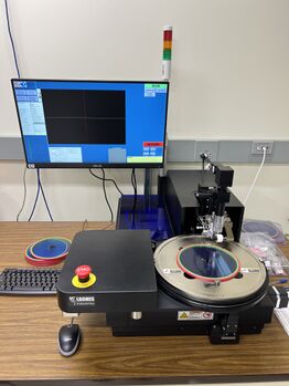
The Loomis LSD-155Lt is a production scribe and break system that can be used for processing large grids, arrays of laser bars, cleaving high quality mirror facets, and dicing wafers.
Detailed Specifications
- Maximum Wafer Size: 4"
- Parts mounted to low tack tape and used in conjunction with 6" plastic rings.
- Automated cut maps at multiple angles (0° and 90° typical)
- ~few micron alignment to on-wafer features.
- Multiple scribe and cleave options including 'scribe and break', 'notch and cleave', and 'peck and cleave'.
- Users should try and follow the 3 to 1 ratio (distance between cleaves should be 3X the thickness of the substrate) although some material like InP and GaAs can occasionally be cleaved closer to 2 to 1.
- Thinning the substrate allows for much easier cleaving and cleave lines closer together.
Operating Procedures
Recipes
- Recipes > Packaging > Wafer Cleaver Recipes (LSD-155LT)
- Wafer thinning is critical, see the Wafer Lapping (Allied 10-1110) tool as well.
