E-Beam 2 (Custom): Difference between revisions
No edit summary |
Updated SOP Rev |
||
| (19 intermediate revisions by 5 users not shown) | |||
| Line 1: | Line 1: | ||
{{ |
{{tool2|{{PAGENAME}} |
||
|picture= |
|picture=IMG 5388.jpg |
||
|type = Vacuum Deposition |
|type = Vacuum Deposition |
||
|super= |
|super= Lee Sawyer |
||
|super2= Mike Barreraz |
|||
|phone=(805)839- |
|phone=(805)839-2123 |
||
|location=Bay 3 |
|location=Bay 3 |
||
|email= |
|email=lee_sawyer@ucsb.edu |
||
|description = Electron-Beam Evaporation System |
|description = Electron-Beam Evaporation System |
||
|manufacturer = Temescal |
|manufacturer = Temescal |
||
| Line 11: | Line 12: | ||
|toolid=8 |
|toolid=8 |
||
}} |
}} |
||
= |
==About== |
||
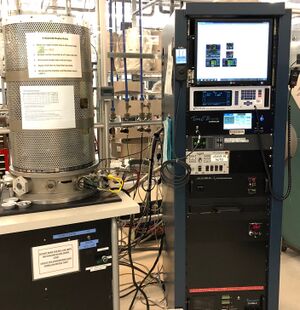
This electron-beam evaporation system is used for the controlled deposition of thin dielectric films. The films are evaporated from a wide variety of solid sources. The most common dielectrics deposited are: SiO<sub>2</sub>, |
This electron-beam evaporation system is used for the controlled deposition of thin dielectric films. The films are evaporated from a wide variety of solid sources. The most common dielectrics deposited are: SiO<sub>2</sub>, ITO, TiO<sub>2</sub>, Ta<sub>2</sub>O<sub>5</sub>, and SrF<sub>2</sub>. Other materials may be evaporated upon request. Oxygen gas can be bled into the system during deposition to try to maintain the stoichiometry during deposition. Fixturing for heating the substrate can also be used. A crystal thickness monitor is used to control the deposition thickness. The dielectrics deposited by this system are typically used for optical coatings (anti-reflective), electrical insulators, and reactive ion etching masks. Samples up to ~ 5" diameter can be placed into this system for evaporation. Typical deposition rates are several Angstroms/second. |
||
= |
==Detailed Specifications== |
||
*Temescal |
*Temescal CV-6SXL 10 kV power supply |
||
*Temescal 4-pocket |
*Temescal 4-pocket Series 260 E-Beam turret source |
||
*Temescal TemEbeam Controller (EBC); controls the high voltage power supply, electron beam position (up to 8 sweep patterns per pocket), and source pocket position |
|||
*Electron beam controller with sweep rate and amplitude control |
|||
*Inficon IC/5 Thin Film Deposition Controller |
|||
*Cryo-pumped system with |
*Cryo-pumped system with low E-7 ultimate base pressure |
||
*Automatic vacuum sequencing |
*Automatic vacuum sequencing via CHA Auto-Tech II |
||
*Crystal thickness monitoring |
*Crystal thickness monitoring |
||
*Sample size: up to 5” |
*Sample size: up to 5” diameter non-heated, 4" diameter heated |
||
| ⚫ | |||
*'''Heated''' sample holder (programmable), sample temps up to 370°C |
|||
| ⚫ | |||
==Documentation== |
|||
<br> |
|||
= Materials Table = |
|||
*[https://wiki.nanofab.ucsb.edu/w/images/8/81/EB2_SOP_Rev_J.pdf E-Beam #2 Standard Operating Procedure] |
|||
For the materials tables, please visit the [[E-Beam_Evaporation_Recipes#Materials_Table_(E-Beam #2)|E-Beam Recipe Page]]. |
|||
==Recipes== |
|||
*[[E-Beam Evaporation Recipes#E-Beam%202%20.28Custom.29|Recipes > Vac. Deposition > '''E-Beam 2 (Custom)''']] |
|||
**Lists the characterized recipes for this machine - other materials may also be used with staff permission. |
|||
Latest revision as of 17:44, 12 February 2026
| ||||||||||||||||||||||||||||||
About
This electron-beam evaporation system is used for the controlled deposition of thin dielectric films. The films are evaporated from a wide variety of solid sources. The most common dielectrics deposited are: SiO2, ITO, TiO2, Ta2O5, and SrF2. Other materials may be evaporated upon request. Oxygen gas can be bled into the system during deposition to try to maintain the stoichiometry during deposition. Fixturing for heating the substrate can also be used. A crystal thickness monitor is used to control the deposition thickness. The dielectrics deposited by this system are typically used for optical coatings (anti-reflective), electrical insulators, and reactive ion etching masks. Samples up to ~ 5" diameter can be placed into this system for evaporation. Typical deposition rates are several Angstroms/second.
Detailed Specifications
- Temescal CV-6SXL 10 kV power supply
- Temescal 4-pocket Series 260 E-Beam turret source
- Temescal TemEbeam Controller (EBC); controls the high voltage power supply, electron beam position (up to 8 sweep patterns per pocket), and source pocket position
- Inficon IC/5 Thin Film Deposition Controller
- Cryo-pumped system with low E-7 ultimate base pressure
- Automatic vacuum sequencing via CHA Auto-Tech II
- Crystal thickness monitoring
- Sample size: up to 5” diameter non-heated, 4" diameter heated
- Heated sample holder (programmable), sample temps up to 370°C
- Oxygen gas MFC for maintaining oxide stoichiometry
Documentation
Recipes
- Recipes > Vac. Deposition > E-Beam 2 (Custom)
- Lists the characterized recipes for this machine - other materials may also be used with staff permission.
