Fluorine ICP Etcher (PlasmaTherm/SLR Fluorine ICP): Difference between revisions
| (8 intermediate revisions by 2 users not shown) | |||
| Line 16: | Line 16: | ||
=About= |
=About= |
||
The system is a Plasma-Therm 770 SLR series system with a loadlock, dedicated to fluorine-based gases (system aka. " |
The system is a Plasma-Therm 770 SLR series system with a loadlock, dedicated to fluorine-based gases (system aka. "FICP"). The system has an Inductively Coupled Plasma (ICP) coil and a capactively coupled substrate RF supply to independently control plasma density and ion energy in the system. Helium back-side cooling is available to keep the sample cool during the etch. The system is fully computer controlled in all aspects of the pumping cycles and process control, and can be programmed by the user. |
||
The system is generally meant for any fluorine-containing etch, which is typically for etching materials like SiO<sub>2</sub>, Si<sub>3</sub>N<sub>4</sub>, Silicon, or other materials with volatile fluoride etch products. |
The system is generally meant for any fluorine-containing etch, which is typically for etching materials like SiO<sub>2</sub>, Si<sub>3</sub>N<sub>4</sub>, Silicon, or other materials with volatile fluoride etch products. |
||
| Line 30: | Line 30: | ||
*1000 W ICP coil power at 2 MHz and 500 W substrate bias at 13.56 MHz plasma generators |
*1000 W ICP coil power at 2 MHz and 500 W substrate bias at 13.56 MHz plasma generators |
||
*C<sub>4</sub>F<sub>8</sub>, SF<sub>6</sub>, O<sub>2</sub>, Ar, N<sub>2,</sub> CHF<sub>3,</sub> CF<sub>4</sub> gases available |
*C<sub>4</sub>F<sub>8</sub>, SF<sub>6</sub>, O<sub>2</sub>, Ar, N<sub>2,</sub> CHF<sub>3,</sub> CF<sub>4</sub> gases available |
||
*He-back-side cooling |
*He-back-side cooling, 10°C std. chuck temp. |
||
*Single 100mm/4-inch wafer handling with physical topside clamp, contacting outer 5mm of wafer. |
*Single 100mm/4-inch wafer handling with physical topside clamp, contacting outer 5mm of wafer. |
||
**Small samples may be mounted with oil or no adhesive, but must be far away from this 5mm edge exclusion zone. |
**Small samples may be mounted with oil or no adhesive, but must be far away from this 5mm edge exclusion zone. |
||
**No photoresist or oil is allowed to contact the clamp, or wafers will get stuck and possibly break in the chamber. |
**No photoresist or oil is allowed to contact the clamp, or wafers will get stuck and possibly break in the chamber. |
||
*Windows-based computer control of process and wafer handling |
*Windows-based computer control of process and wafer handling |
||
**Easy to chain recipes via "Batch" programming, eg. ''SiO2 Etch / Si Etch / PR strip'' in a single load. |
|||
*[[Laser Etch Monitoring|Laser endpoint monitoring]] with camera and simulation software, for repeatable etching - see: [[Laser Etch Monitoring|Intellemetrics LEP 500]] |
*[[Laser Etch Monitoring|Laser endpoint monitoring]] with camera and simulation software, for repeatable etching - see: [[Laser Etch Monitoring|Intellemetrics LEP 500]] |
||
| Line 56: | Line 57: | ||
===Process Control Data=== |
===Process Control Data=== |
||
We have two different EtchCals on this tool: |
|||
Plots of etch calibrations can be found on the following spreadsheets: |
|||
==== SiO<sub>2</sub> Etching ==== |
|||
''We have found that SiO<sub>2</sub> etching is fairly insensitive to chamber condition.'' |
|||
| ⚫ | |||
| ⚫ | *[https://docs.google.com/spreadsheets/d/15hYkCqL3UNNayt4sXrvVi4mBj-OSdnF7PE29mQW9AEY/edit#gid=1804752281 SiO<sub>2</sub> Etching with CHF<sub>3</sub>/CF<sub>4</sub> - '''Plots'''][[File:FL-ICP Process Control Data Example.jpg|alt=example of Process Control Charts|none|thumb|242x242px|[https://docs.google.com/spreadsheets/d/15hYkCqL3UNNayt4sXrvVi4mBj-OSdnF7PE29mQW9AEY/edit#gid=1804752281 Click for Process Control Charts]|link=https://docs.google.com/spreadsheets/d/15hYkCqL3UNNayt4sXrvVi4mBj-OSdnF7PE29mQW9AEY/edit#gid=1804752281]] |
||
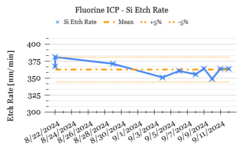
==== Si Etching ==== |
|||
''This Si etch is much more sensitive to chamber condition, allowing us to detect chamber contamination faster.'' |
|||
| ⚫ | |||
| ⚫ | *[https://docs.google.com/spreadsheets/d/15hYkCqL3UNNayt4sXrvVi4mBj-OSdnF7PE29mQW9AEY/edit#gid=1804752281 SiO<sub>2</sub> Etching with |
||
*SiVertHFv2 - Full Wafer Si etching with ~50% open area |
|||
*[https://docs.google.com/spreadsheets/d/15iRs-JhfgkMto5rZVtG0hJjcLMiHy039_ahv2nus0UQ/edit?gid=0#gid=0 Si Etching with C<sub>4</sub>F<sub>8</sub>/SF<sub>6</sub>/CF<sub>4</sub> - '''Etch Data'''] |
*[https://docs.google.com/spreadsheets/d/15iRs-JhfgkMto5rZVtG0hJjcLMiHy039_ahv2nus0UQ/edit?gid=0#gid=0 Si Etching with C<sub>4</sub>F<sub>8</sub>/SF<sub>6</sub>/CF<sub>4</sub> - '''Etch Data'''] |
||
*[https://docs.google.com/spreadsheets/d/15iRs-JhfgkMto5rZVtG0hJjcLMiHy039_ahv2nus0UQ/edit?gid=1804752281#gid=1804752281 Si Etching with C<sub>4</sub>F<sub>8</sub>/SF<sub>6</sub>/CF<sub>4</sub> - '''Plots'''][[File:FICP-Si.png|alt=example of Process Control Charts|none|thumb|242x242px|[https://docs.google.com/spreadsheets/d/15iRs-JhfgkMto5rZVtG0hJjcLMiHy039_ahv2nus0UQ/edit?gid=1804752281#gid=1804752281 Click for Process Control Charts]|link=https:// |
*[https://docs.google.com/spreadsheets/d/15iRs-JhfgkMto5rZVtG0hJjcLMiHy039_ahv2nus0UQ/edit?gid=1804752281#gid=1804752281 Si Etching with C<sub>4</sub>F<sub>8</sub>/SF<sub>6</sub>/CF<sub>4</sub> - '''Plots'''][[File:FICP-Si.png|alt=example of Process Control Charts|none|thumb|242x242px|[https://docs.google.com/spreadsheets/d/15iRs-JhfgkMto5rZVtG0hJjcLMiHy039_ahv2nus0UQ/edit?gid=1804752281#gid=1804752281 Click for Process Control Charts]|link=https://docs.google.com/spreadsheets/d/15iRs-JhfgkMto5rZVtG0hJjcLMiHy039_ahv2nus0UQ/edit?gid=1804752281#gid=1804752281]] |
||
Latest revision as of 23:29, 12 November 2025
| ||||||||||||||||||||||||||||||||

About
The system is a Plasma-Therm 770 SLR series system with a loadlock, dedicated to fluorine-based gases (system aka. "FICP"). The system has an Inductively Coupled Plasma (ICP) coil and a capactively coupled substrate RF supply to independently control plasma density and ion energy in the system. Helium back-side cooling is available to keep the sample cool during the etch. The system is fully computer controlled in all aspects of the pumping cycles and process control, and can be programmed by the user.
The system is generally meant for any fluorine-containing etch, which is typically for etching materials like SiO2, Si3N4, Silicon, or other materials with volatile fluoride etch products.
The fixturing is configured for 4" diameter Si wafers and uses a ceramic clamp on the outer ~5mm of the 100mm wafer to hold the sample on the RF chuck.
Smaller samples can be mounted onto 100mm carrier wafers, either with no adhesive (sample temperature will be higher), or with Santovac oil for better thermal cooling. However, great care must be taken to ensure no oil, photoresist or small pieces are placed on the outer 5mm of the carrier wafer, as the ceramic clamp will physically press on this outer region, potentially causing stiction or wafer breakage if foreign or sticky substances are in those regions.
The in-situ laser monitor installed on the chamber allows for repeatable etches and endpoint detection via continuous optical monitoring of the wafer reflectivity in a user-determined location, through a porthole on the chamber.
Detailed Specifications
- 1000 W ICP coil power at 2 MHz and 500 W substrate bias at 13.56 MHz plasma generators
- C4F8, SF6, O2, Ar, N2, CHF3, CF4 gases available
- He-back-side cooling, 10°C std. chuck temp.
- Single 100mm/4-inch wafer handling with physical topside clamp, contacting outer 5mm of wafer.
- Small samples may be mounted with oil or no adhesive, but must be far away from this 5mm edge exclusion zone.
- No photoresist or oil is allowed to contact the clamp, or wafers will get stuck and possibly break in the chamber.
- Windows-based computer control of process and wafer handling
- Easy to chain recipes via "Batch" programming, eg. SiO2 Etch / Si Etch / PR strip in a single load.
- Laser endpoint monitoring with camera and simulation software, for repeatable etching - see: Intellemetrics LEP 500
Documentation
- How to restart software on Plasma-Therm Cortex Software
- Laser Monitor procedures
- How to edit recipe
- Cleaning rules
- Manual Edge-Bead Removal Techniques - 5mm of outer edge must be free of photoresist, use these techniques to accomplish that for full wafers.
Recipes
- Recipes > Dry Etching > PlasmaTherm/SLR Fluorine Etcher
- Starting point recipes for the FL-ICP, including SiO2 and Si etches.
- Process Control Data records "calibration" etches to test tool performance.
- You can see a full list of all tools and all materials able to be etched on our Dry Etching Recipes Table.
Process Control Data
We have two different EtchCals on this tool:
SiO2 Etching
We have found that SiO2 etching is fairly insensitive to chamber condition.
- SiO2 Etching with CHF3/CF4 - Etch Data
- SiO2 Etching with CHF3/CF4 - Plots
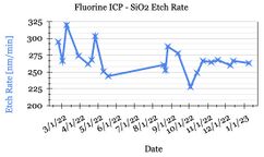
Click for Process Control Charts
Si Etching
This Si etch is much more sensitive to chamber condition, allowing us to detect chamber contamination faster.