Resistivity Mapper (CDE RESMAP): Difference between revisions
Jump to navigation
Jump to search
Content deleted Content added
No edit summary |
added CSV export |
||
| Line 10: | Line 10: | ||
|materials = |
|materials = |
||
}} |
}} |
||
= |
=About= |
||
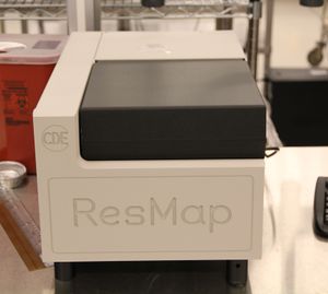
The CDE Resmap 4 point resistivity mapper is used for measuring resistivity across the wafer for substrates and thin films deposited in the facility. The system can do automated resistivity mapping for pieces to 8 inch wafers. |
The CDE Resmap 4 point resistivity mapper is used for measuring resistivity across the wafer for substrates and thin films deposited in the facility. The system can do automated resistivity mapping for pieces to 8 inch wafers. |
||
The resistivity range is 2 mOhm/Square to 5 MOhm/square. Contour plots, 3D plots, histograms, data exporting are supported from the Windows XP based control system. |
The resistivity range is 2 mOhm/Square to 5 MOhm/square. Contour plots, 3D plots, histograms, data exporting are supported from the Windows XP based control system. |
||
== |
==Instructions== |
||
* |
*[[CDE ResMap Quick-Start instructions]] |
||
*System can export CSV files - contact supervisor for instructions. |
|||
Revision as of 19:08, 1 November 2021
|
About
The CDE Resmap 4 point resistivity mapper is used for measuring resistivity across the wafer for substrates and thin films deposited in the facility. The system can do automated resistivity mapping for pieces to 8 inch wafers.
The resistivity range is 2 mOhm/Square to 5 MOhm/square. Contour plots, 3D plots, histograms, data exporting are supported from the Windows XP based control system.
Instructions
- CDE ResMap Quick-Start instructions
- System can export CSV files - contact supervisor for instructions.
