Surface Analysis (KLA/Tencor Surfscan): Difference between revisions
Jump to navigation
Jump to search
Content deleted Content added
→Documentation: added info, and inof on LPC wafers |
|||
| Line 30: | Line 30: | ||
**''You must provide your own 2/3-inch Cassette.'' |
**''You must provide your own 2/3-inch Cassette.'' |
||
*[https://wiki.nanofab.ucsb.edu/w/images/4/4e/SURFSCAN_6200_Small_substrates.pdf Surfscan 6200 Small samples] * |
*[https://wiki.nanofab.ucsb.edu/w/images/4/4e/SURFSCAN_6200_Small_substrates.pdf Surfscan 6200 Small samples] * |
||
*[https://wiki.nanofab.ucsb.edu/w/images/a/a7/SURFSCAN_6200_122123_small_substrates.pdf Surfscan 6200 Small samples, and 2inch and 3inch wafers] * |
|||
**''You must water-mount your pieces to a 4-inch wafer.'' |
**''You must water-mount your pieces to a 4-inch wafer.'' |
||
*[[Wafer scanning process traveler|Wafer Particle Count - Process Traveler]] |
*[[Wafer scanning process traveler|Wafer Particle Count - Process Traveler]] |
||
**''This is the procedure Staff uses to calibrate particle counts on our deposition tools.'' |
**''This is the procedure Staff uses to calibrate particle counts on our deposition tools.'' |
||
https://wiki.nanofab.ucsb.edu/w/images/a/a7/SURFSCAN_6200_122123_small_substrates.pdf |
|||
===Other Documentation=== |
===Other Documentation=== |
||
Revision as of 00:41, 5 January 2024
| ||||||||||||||||||||||||||
About
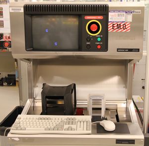
This system uses a laser-based scattering method to count size and distribution of particles (or other scattering defects) on a flat wafer surface.
It can scan wafers in size from 4 to 8 inches. Piece-parts are more difficult but can be scanned with a custom recipe.
4-inch wafers are the most standard size to measure.
For measuring very low particle counts accurately, purchase "low particle count" (LPC) wafers from a Silicon wafer vendor, and keep the wafers in the case and clean at all times until use.
Documentation
Operating Procedures
- Surfscan 6200 8inch wafers *
- Surfscan 6200 6inch wafers *
- Surfscan 6200 4inch wafers *
- Surfscan 6200 2 and 3inch wafers *
- You must provide your own 2/3-inch Cassette.
- Surfscan 6200 Small samples *
- Surfscan 6200 Small samples, and 2inch and 3inch wafers *
- You must water-mount your pieces to a 4-inch wafer.
- Wafer Particle Count - Process Traveler
- This is the procedure Staff uses to calibrate particle counts on our deposition tools.
https://wiki.nanofab.ucsb.edu/w/images/a/a7/SURFSCAN_6200_122123_small_substrates.pdf
Other Documentation
- Operations Manual
- For detailed measurement info, it is highly recommended that you read the manual.
Examples
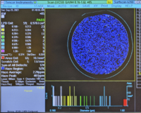
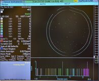
| Gain 4: Small Particles
(0.160µm – 1.60µm) |
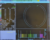
Gain 2: Large Particles
(1.60µm – 28.0µm) |
|---|---|
|
|
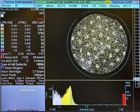
| Gain 4: Small Particles
(0.160µm – 1.60µm) |
Gain 2: Large Particles
(1.60µm – 28.0µm) |
|---|---|
|
|
