Oxford ICP Etcher (PlasmaPro 100 Cobra): Difference between revisions
→Recipes: promoted recipes page to larger heading level |
|||
| Line 63: | Line 63: | ||
=== [[ICP Etching Recipes#Process Control Data .28Oxford ICP Etcher.29|Process Control Data]] === |
=== [[ICP Etching Recipes#Process Control Data .28Oxford ICP Etcher.29|Process Control Data]] === |
||
''Click above for calibration etch data for verifying tool performance over time.'' |
''Click above for calibration etch data for verifying tool performance over time.'' |
||
=== High-Temp (200°C) InP Etch Process === |
|||
* InP Ridge Etch 200°C - ''Noah Dutra & Fatt Foong, 2025-08-12'' |
|||
** Etch rates ~2 um/min, Selectivity to SiO2 ~ 30:1, Sidewalls ~90° |
|||
** Very dependent on open area, more area => lower E.R.s |
|||
** Cal Sample: ~1cm sample etched with 1 quarter of blank 50mm InP seasoning wafer placed '''without''' mounting adhesive on blank Silicon carriers (rough side up). |
|||
** Recipe: Cl2/H2/Ar - 200°C |
|||
==== Process Control: High-Temp (200°C) InP Etch ==== |
|||
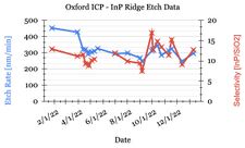
[[/wiki/File:200C_InP.png|link=https://docs.google.com/spreadsheets/d/1LE5Cug9uJFYEwu0ZsNsp0W1dTRzcO2EKFhC0wu3w0n4/edit?gid=1804752281#gid=1804752281|alt=example SPC chart for Oxford ICP Etcher|thumb|218x218px|Click for Process Control Charts for 200°C InP Etch]] |
|||
''Calibration / Process testing data taken using the "InP Ridge Etch" process: Cl2/H2/Ar @ 200°C, 1cm piece with ~50% SiO2 hardmask.'' |
|||
* "Std InP Ridge Etch" Cl<sub>2</sub>/H<sub>2</sub>/Ar 200°C - '''Etch Data Tables''' |
|||
* "Std InP Ridge Etch" Cl<sub>2</sub>/H<sub>2</sub>/Ar 200°C - '''Plots''' |
|||
==== [https://docs.google.com/spreadsheets/d/1cEUB7K5BAg9N4vp3rPZw7g0orFkxeQmRkX34Fb4eZco/edit#gid=1804752281 Std InP Ridge Etch: Cl<sub>2</sub>/CH<sub>4</sub>/H<sub>2</sub>/60°C] ==== |
==== [https://docs.google.com/spreadsheets/d/1cEUB7K5BAg9N4vp3rPZw7g0orFkxeQmRkX34Fb4eZco/edit#gid=1804752281 Std InP Ridge Etch: Cl<sub>2</sub>/CH<sub>4</sub>/H<sub>2</sub>/60°C] ==== |
||
''Calibration / Process testing data taken using the "InP Ridge Etch" process: Cl2/CH4/H2 @ 60°C, 1cm piece with ~50% SiO2 hardmask.'' |
''Calibration / Process testing data taken using the "InP Ridge Etch" process: Cl2/CH4/H2 @ 60°C, 1cm piece with ~50% SiO2 hardmask.'' |
||
<u>''No longer calibrating 60°C process as of 05-2025.''</u> |
|||
*[https://docs.google.com/spreadsheets/d/1cEUB7K5BAg9N4vp3rPZw7g0orFkxeQmRkX34Fb4eZco/edit?usp=sharing "Std InP Ridge Etch" Cl<sub>2</sub>/CH<sub>4</sub>/H<sub>2</sub>/60°C - '''Etch Data Tables'''] |
*[https://docs.google.com/spreadsheets/d/1cEUB7K5BAg9N4vp3rPZw7g0orFkxeQmRkX34Fb4eZco/edit?usp=sharing "Std InP Ridge Etch" Cl<sub>2</sub>/CH<sub>4</sub>/H<sub>2</sub>/60°C - '''Etch Data Tables'''] |
||
| Line 71: | Line 88: | ||
==== GaN Etch (Cl2/BCl3/Ar/200°C) ==== |
==== GaN Etch (Cl2/BCl3/Ar/200°C) ==== |
||
Recipe: '' |
CURRENT Recipe: ''6" STD GaN Etch - BCl3/Cl2/Ar - 200C (Public)'', on 1cm x 1cm with 6" configuration, ''~850nm deep GaN Etch with Cl2/BCl3/Ar at 200°C. GaN-on-Sapphire substrate with SiN mask.'' |
||
* This recipe is the same as the 4" (old) Std recipe but with 140% flows. Current recipe is 200c, 4.5mT, 700W/50W, Cl2/Ar/BCl3 = 49.1/16.4/12.2sccm. |
|||
* CURRENT 6" configuration: GaN Etching with Cl2/BCl3/Ar at 200°C - Etch Data |
|||
* CURRENT 6" configuration: GaN Etching with Cl2/BCl3/Ar at 200°C - Plots |
|||
OLD Recipe: ''Std GaN Etch - BCl3/Cl2/Ar - 200C (Public)'', on 1cm x 1cm with 4" configuration, ''~1.2µm deep GaN etch with Cl2/BCl3/Ar at 200°C.'' Sapphire substrate with SiO2 mask for GaN. |
|||
*[https://docs.google.com/spreadsheets/d/1Pk8VwZlZ2lUf3aL9J2El5ZygqHY040TX3ZAMwa33LpE/edit?gid=0#gid=0 GaN Etching with Cl2/BCl3/Ar at 200°C - Etch Data] |
*[https://docs.google.com/spreadsheets/d/1Pk8VwZlZ2lUf3aL9J2El5ZygqHY040TX3ZAMwa33LpE/edit?gid=0#gid=0 GaN Etching with Cl2/BCl3/Ar at 200°C - Etch Data] |
||
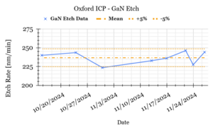
*[https://docs.google.com/spreadsheets/d/1Pk8VwZlZ2lUf3aL9J2El5ZygqHY040TX3ZAMwa33LpE/edit?gid=507237279#gid=507237279 GaN Etching with Cl2/BCl3/Ar at 200°C - Plots][[File:GaN SPC.png|alt=example of Process Control Charts|none|thumb|[https://docs.google.com/spreadsheets/d/1Pk8VwZlZ2lUf3aL9J2El5ZygqHY040TX3ZAMwa33LpE/edit?gid=507237279#gid=507237279 Click for Process Control Charts]|link=https://docs.google.com/spreadsheets/d/1Pk8VwZlZ2lUf3aL9J2El5ZygqHY040TX3ZAMwa33LpE/edit?gid=507237279#gid=507237279]]<hr style="height:5px"> |
*[https://docs.google.com/spreadsheets/d/1Pk8VwZlZ2lUf3aL9J2El5ZygqHY040TX3ZAMwa33LpE/edit?gid=507237279#gid=507237279 GaN Etching with Cl2/BCl3/Ar at 200°C - Plots][[File:GaN SPC.png|alt=example of Process Control Charts|none|thumb|[https://docs.google.com/spreadsheets/d/1Pk8VwZlZ2lUf3aL9J2El5ZygqHY040TX3ZAMwa33LpE/edit?gid=507237279#gid=507237279 Click for Process Control Charts]|link=https://docs.google.com/spreadsheets/d/1Pk8VwZlZ2lUf3aL9J2El5ZygqHY040TX3ZAMwa33LpE/edit?gid=507237279#gid=507237279]]<hr style="height:5px"> |
||
Revision as of 18:55, 12 February 2026
| ||||||||||||||||||||||||||||||

About
The Oxford PlasmaPro 100 Cobra 300 is intended for etching InP-based, GaAs-baased and GaN-based epitaxies, in addition to Atomic Layer Etching (ALE) processes. The system has a load lock, wide temperature range with rapid heating/cooling, Inductively Coupled Plasma (ICP) coil and a capactively coupled substrate HF (13.56MHz) The fixturing is configured for 4" diameter Si wafers and uses a clamp to hold the sample on the RF chuck. Small pieces may be placed on Silicon carrier wafers, with or without mounting adhesive. Helium back-side cooling is used to keep the sample cool during the etch, but pieces do heat up when placed on carriers.
The in-situ laser monitor installed on this system allows for repeatable etches and endpoint detection via continuous optical monitoring of the wafer reflectivity in a user-determined location, through a porthole on the chamber. The system also has an in situ optical emission monitor for plasma spectroscopy, utilized for chamber clean endpoint detection.
Detailed Specifications
- Temperature Range: –150°C to +400°C
- Gases Available: CH4, H2, Ar, Cl2, BCl3, SF6, SiCl4, O2, N2
- ICP Power (max): 3000 W
- RF Power (max): 600 W
- He-back-side cooling
- 100mm wafer held down with ceramic clamp., single-load
- Users may place pieces onto carrier wafer with or without adhesive. Standard recipes use no adhesive.
- Pieces must be >7mm from edge of carrier to avoid wafer-clamping mechanism.
- Windows-based Cortex software control of process and wafer handling
- Allowed Materials:
- InP-based epitaxies - qualified and ready
- GaAs-baased epitaxies - starter recipe is available
- GaN-based epitaxies - starter recipe is available
- GaSb-based epitaxies - starter recipe is available
- Atomic Layer Etching on select materials - starter recipe is available
- Standard masking materials include:
- SiO2
- Si3N4
- photoresist (at << 100°C).
Other materials can be exposed to the chamber only with staff approval.
- Laser monitoring with camera and etch simulation software: Intellemetrics LEP 500
- Optical Emission Spectroscopy (Ocean Optics) for endpoint detection of chamber cleans & etches - integrated into Oxford software
Documentation
- Oxford PlasmaPro Operating Instructions
- Includes "Travelers" and post-cleaning for each type of standard etch (InP, GaAs, GaN)
- Laser Etch Monitoring procedures
- Online Training Video:
- Oxford Cobra 300 Training
- Important: This video is for reference only, and does not give you authorization to use the tool. You must be officially authorized by the supervisor before using this machine.
Recipes
Oxford PlasmaPro Recipes ← Recipes specific to this tool.
- All Dry Etching Recipes - use this list to see other options for dry etching various materials.
Process Control Data
Click above for calibration etch data for verifying tool performance over time.
High-Temp (200°C) InP Etch Process
- InP Ridge Etch 200°C - Noah Dutra & Fatt Foong, 2025-08-12
- Etch rates ~2 um/min, Selectivity to SiO2 ~ 30:1, Sidewalls ~90°
- Very dependent on open area, more area => lower E.R.s
- Cal Sample: ~1cm sample etched with 1 quarter of blank 50mm InP seasoning wafer placed without mounting adhesive on blank Silicon carriers (rough side up).
- Recipe: Cl2/H2/Ar - 200°C
Process Control: High-Temp (200°C) InP Etch
link=https://docs.google.com/spreadsheets/d/1LE5Cug9uJFYEwu0ZsNsp0W1dTRzcO2EKFhC0wu3w0n4/edit?gid=1804752281#gid=1804752281|alt=example SPC chart for Oxford ICP Etcher|thumb|218x218px|Click for Process Control Charts for 200°C InP Etch Calibration / Process testing data taken using the "InP Ridge Etch" process: Cl2/H2/Ar @ 200°C, 1cm piece with ~50% SiO2 hardmask.
- "Std InP Ridge Etch" Cl2/H2/Ar 200°C - Etch Data Tables
- "Std InP Ridge Etch" Cl2/H2/Ar 200°C - Plots
Std InP Ridge Etch: Cl2/CH4/H2/60°C
Calibration / Process testing data taken using the "InP Ridge Etch" process: Cl2/CH4/H2 @ 60°C, 1cm piece with ~50% SiO2 hardmask.
No longer calibrating 60°C process as of 05-2025.
- "Std InP Ridge Etch" Cl2/CH4/H2/60°C - Etch Data Tables
- "Std InP Ridge Etch" Cl2/CH4/H2/60°C - Plots
Click for Process Control Charts
GaN Etch (Cl2/BCl3/Ar/200°C)
CURRENT Recipe: 6" STD GaN Etch - BCl3/Cl2/Ar - 200C (Public), on 1cm x 1cm with 6" configuration, ~850nm deep GaN Etch with Cl2/BCl3/Ar at 200°C. GaN-on-Sapphire substrate with SiN mask.
- This recipe is the same as the 4" (old) Std recipe but with 140% flows. Current recipe is 200c, 4.5mT, 700W/50W, Cl2/Ar/BCl3 = 49.1/16.4/12.2sccm.
- CURRENT 6" configuration: GaN Etching with Cl2/BCl3/Ar at 200°C - Etch Data
- CURRENT 6" configuration: GaN Etching with Cl2/BCl3/Ar at 200°C - Plots
OLD Recipe: Std GaN Etch - BCl3/Cl2/Ar - 200C (Public), on 1cm x 1cm with 4" configuration, ~1.2µm deep GaN etch with Cl2/BCl3/Ar at 200°C. Sapphire substrate with SiO2 mask for GaN.