Sputtering Recipes
Back to Vacuum Deposition Recipes. R1
Sputter 3 (AJA ATC 2000-F)
Please see the SignupMonkey Page for a list of currently installed targets.
Tips & Tricks
Ignition Issues
It is somewhat common that you might have a plasma ignition failure at some point. Common remedies for this are to increase the chamber pressure just for the ignition step, then drop dow to the process pressure in the PreClean and/or Dep step. For example, set the ignition step pressure to 10mTorr or 30mT, then during deposition decrease the pressure to 3mTorr and the plasma will stay lit.
Materials Table (Sputter 3)
The recipes below are given as starting points from data obtained in the nanofab. For critical depositions, calibrations are recommended.
| Material | P(mT) | Pow(W) | Sub(W) | T(C) | Ar | N2 | O2 | Height-Tilt(mm) | Rate(nm/min) | Stress(MPa) | Rs(uOhm-cm) | n@633nm | k@633nm | Target Consumed Lower Limit | Data Below | Comment |
|---|---|---|---|---|---|---|---|---|---|---|---|---|---|---|---|---|
| Au | - | - | - | - | - | - | - | - | - | - | - | - | - | Set: 200 W
Read: 400 VDC |
no | |
| Al2O3 | 3 | 200 (RF2) | off | 20 | 30 | 1.5 | 1.52"-4mm | 5.32 | 1.6478 | 0 | no | Demis D. John | ||||
| Co | 10(5) | 200 | 0 | 20 | 25 | 0 | 0 | 25-9 | 2.3 | - | - | - | - | yes | Alex K | |
| Cr | 5 | 200 | 0 | 20 | 25 | 0 | 0 | 44-4 | 6.84 | - | - | - | - | no | Brian | |
| Cu | 1.5 | 50(395v) | 0 | 20 | 25 | 0 | 0 | 25-9 | 4.15 | - | - | - | - | no | Ning | |
| Cu | 5 | 150(~490v) | 0 | 20 | 15 | 0 | 0 | 0.82"-9 | 8 | - | - | - | - | yes | Ning | |
| Fe | 10(5) | 200 | 0 | 20 | 25 | 0 | 0 | 25-9 | 1.25 | - | - | - | - | No | Alex K | |
| Mo | 3 | 200 | 0 | 20 | 25 | 0 | 0 | 44-4 | 13.15 | - | - | - | - | yes | Ning | |
| Ni | 5 | 150 | 0 | 20 | 25 | 0 | 0 | 44-4 | 5.23 | - | - | - | - | yes | Ning | |
| Ni | 5 | 150 | 0 | 20 | 25 | 0 | 0 | 25-9 | 1.82 | - | - | - | - | yes | Ning | |
| Ni | 5 | 75 | 0 | 20 | 25 | 0 | 0 | 44-4 | 2.50 | - | - | - | - | yes | Ning | |
| Ni | 3 | 200 | 0 | 20 | 25 | 0 | 0 | 44-4 | 9.4 | - | - | - | - | yes | Ning | |
| Ni | 1.5 | 50(399v) | 0 | 20 | 25 | 0 | 0 | 25-9 | 0.96 | - | - | - | - | no | Ning | |
| Pt | 3 | 50 | 0 | 20 | 25 | 0 | 0 | 0.82"-9 | 2.9 | - | - | - | - | no | Ning | |
| Si | 8 | 250 | 0 | 25 | 25 | 0 | 0 | 15-3 | 1.4 | - | - | - | - | no | Gerhard - ramp 2W/s - 3% Unif 4" wafer | |
| SiN | 3 | 200 | 10 | 20 | 25 | 3 | 0 | 25-9 | 1.56 | - | - | 1.992 | - | yes | Brian | |
| SiN | 3 | 250 | 10 | 20 | 25 | 2.5 | 0 | 25-9 | 2.1 | - | - | 2.06 | - | yes | Brian | |
| SiO2 | 3 | 200 | 10 | 20 | 25 | 0 | 3 | 25-9 | 3.68 | - | - | 1.447 | - | yes | Brian | |
| SiO2 | 3 | 200 | 10 | 20 | 25 | 0 | 5 | 45-3 | 2.60 | - | - | 1.471 | - | yes | Brian | |
| SiO2 | 3 | 250 | 10 | 20 | 25 | 0 | 2.5 | 25-9 | 4.3 | - | - | 1.485 | - | yes | Brian | |
| Ta | 5 | 150 | 0 | 20 | 25 | 0 | 0 | 44-4 | 9.47 | - | - | - | - | yes | Ning | |
| Ta | 5 | 75 | 0 | 20 | 25 | 0 | 0 | 44-4 | 5.03 | - | - | - | - | yes | Ning | |
| Ti | 3 | 100 | 0 | 20 | 25 | 0 | 0 | 25-9 | 1.34 | - | - | - | - | yes | Ning | |
| SampleClean-NativeSiO2 | 10 | 0 | 18 | 20 | 25 | 0 | 0 | 44-4 | - | - | - | - | - | yes | 150Volts 5 min |
Height Conversion for Older Recipes
Old recipes using the manual Height setting in millimeters can be converted to the new programmatic settings in inches as follows:
| Old (mm) | New (inches) | Typical Gun Tilt (mm) |
|---|---|---|
| 15 | ||
| 25 | 0.82 | 9 |
| 44 | 1.52 | 4 |
Interpolation plot can be found here.
Fe and Co Deposition (Sputter 3)
Cu Deposition (Sputter 3)
Mo Deposition (Sputter 3)
Ni and Ta Deposition (Sputter 3)
SiO2 Deposition (Sputter 3)
SiN Deposition (Sputter 3)
Ti Deposition (Sputter 3)
Sputter 4 (AJA ATC 2200-V)
Please see the SignupMonkey page for a list of currently installed targets.
Materials Table (Sputter 4)
The recipes below are given as starting points from data obtained in the nanofab. For critical depositions, calibrations are recommended.
| Material | P(mT) | Power Source | Pow(W) | Sub(W) | T(C) | Ar | N2 | O2 | Height-Tilt(mm) | Rate(nm/min) | Stress(MPa) | Rs(uOhm-cm) | n@633nm | k@633nm | Data Below | Comment |
|---|---|---|---|---|---|---|---|---|---|---|---|---|---|---|---|---|
| Al | 5 | 200 | 0 | 20 | 45 | 0 | 0 | H2.75-T5 | 4.4 | - | - | - | - | Yes | Ning Cao | |
| Al2O3 | 3 | RF4-Sw1 | 200 | 0 | 20 | 30 | 0 | 1.5 | H2.75-T5 | 5.1 | 1.64202 | 0 | partial | Demis D. John | ||
| Au | 5 | 200 | 0 | 20 | 45 | 0 | 0 | H1-T10 | 17.7 | - | - | - | - | Yes | Ning Cao | |
| Au | 10 | 200 | 0 | 20 | 45 | 0 | 0 | H2.75-T5 | 35.5 | - | - | - | - | Yes | Demis: 200W rate (Max for Au) 2022-08-03 | |
| Cu | 5 | 150 | 0 | 20 | 30 | 0 | 0 | H0.82-T9 | 6.7 | No (SEM available) | Ning Cao | |||||
| Nb | 4 | 250 | 0 | 20 | 30 | 0 | 0 | H2.00-T7 | 7.5 | - | - | - | - | No | ||
| Pt | 5 | 200 | 0 | 20 | 45 | 0 | 0 | H2.75-T5 | 7.4 | - | - | - | - | Yes | Ning Cao | |
| Pt | 3 | 50(439V) | 0 | 20 | 45 | 0 | 0 | H2.75-T5 | 3.9 | - | - | - | - | Yes | Ning Cao | |
| Ru | 3 | 200 | 45 | H2.75-T4 | ~10 | Yes | Ning Cao | |||||||||
| Ti | 10 | 200 | 0 | 20 | 45 | 0 | 0 | H2.75-T5 | 2.3 | - | - | - | - | Yes | Ning Cao | |
| TiN | 3 | 150 | 110V | 20 | 48.25 | 1.75 | 0 | H2.5-T5 | 2 | - | 60 | - | - | No | ||
| TiO2 | 3 | 250(RF:450V) | 0 | 20 | 45 | 0 | 3 | H2.75-T5 | 4.3 | - | - | - | Yes | Ning Cao | ||
| TiW | 4.5 | 200 | 0 | 20 | 45 | 0 | 0 | H1-T10 | 4.7 | - | - | - | - | Yes | Ning Cao | |
| TiW | 4.5 | 300 | 0 | 75 | 45 | 0 | 0 | H2.75-T5 | 9.5 | -150 to 150 | 60 | - | - | Yes | 10%Ti by Wt | |
| W | 3 | 300 | 0 | 50 | 45 | 0 | 0 | H2.75-T5 | 11.5 | -150 to 150 | 11 | - | - | Yes | Jeremy Watcher |
Au Deposition (Sputter 4)
Al Deposition (Sputter 4)
Al2O3 Deposition (Sputter 4)
- Rate: 5.134 nm/min
- Cauchy Refractive Index Params (fit from λ=190-1700nm, indicating transparency over this range)
- A = 1.626
- B = 5.980E-3
- C = 1.622E-4
Pt Deposition (Sputter 4)
Ru Deposition (Sputter 4)
- Ruthenium Hardmask for SiO2 Etching - Full Process Traveler by Ning Cao
- Deposition Rate ~10nm/min
- See Fluorine-ICP > SiO2 Etching page for more info.
Ti-Au Deposition (Sputter 4)
TiO2 Deposition (Sputter 4)
TiW Deposition (Sputter 4)
W-TiW Deposition (Sputter 4)
Sputter 5 (AJA ATC 2200-V)
Please see the SignupMonkey page for a list of currently installed targets.
Materials Table (Sputter 5)
The recipes below are given as starting points from data obtained in the nanofab. For critical depositions, calibrations are recommended.
| Material | P(mT) | Power Source | Pow(W) | Sub(V) | T(C) | Ar | N2 | O2 | Height-Tilt(mm) | Rate(nm/min) | Stress(MPa) | Rs(uOhm-cm) | Rq(nm) | n@633nm | k@633nm | LPDb/LPDa* | Data Below | Comment |
|---|---|---|---|---|---|---|---|---|---|---|---|---|---|---|---|---|---|---|
| Al | 5 | 250 | 0 | 20 | 45 | 0 | 0 | H1-T10 | 2.5 | 22 | No (SEM available) | Ning | ||||||
| Al2O3 | 1.5 | DC5-SW1 | 150 | - | - | 45 | - | 5 | H2.75-T5 | 5.3 | ? | ? | ? | 1.641 | - | ? | No | Demis 2018-04-13 |
| Cr | 5.0 | RF | 200 | ~345 | 20 | 45 | H2.75-T5 | 4.47 | No | BT 2024-07-02 | ||||||||
| Pt | 3.0 | 200(507v) | - | - | 45 | - | - | H1-T10 | 7.03 | ? | ? | ? | 2.068 | 4.951 | ? | No | Ning 2021-09-27 | |
| SiO2 | 3 | 250 | 120 | 20 | 45 | 0 | 2 | H1.0-T10 | 2.32 | - | - | 1.49 | - | 153/6384 | No | Biljana | ||
| SiO2 | 3 | 250 | 120 | 20 | 45 | 0 | 4.5 | H1.0-T10 | 2.29 | -515 | - | 0.210 | 1.49 | 138/4445 | No ( AFM available) | Biljana | ||
| SiO2 | 3 | 250 | 120 | 20 | 45 | 0 | 6 | H1.0-T10 | 2.32 | - | - | 1.49 | - | 27/1515 | Yes | Biljana | ||
| Ti | 3.0 | 200(374v) | - | - | 45 | - | - | H1-T10 | 2.52 | ? | ? | ? | 2.679 | 1.853 | ? | No | Ning 2021-09-27 |
*LPD: light particle detection:
- LPDb: light particle detection before deposition
- LPDa: light particle detection after deposition
SiO2 Deposition (Sputter 5)
Ion Beam Deposition (Veeco NEXUS)
Ion-Beam Assisted Deposition - high density reactive sputtering for dielectric film stacks, with angled/rotating fixtures.
- Method to calibrate multi-layer optical films: For example, for calibrating and depositing Multi-layer DBR gratings, Anti-Reflection coatings etc.
IBD Process Control Plots - Plots of all process control data.
SiO2 deposition (IBD)
- SiO2 [IBD] Standard Recipe - "1_SiO2_dep"
- SiO2 [IBD] Process Control Data
- SiO2 [IBD] Historical Data - Before Oct. 2021
SiO2 Thin-Film Properties (IBD)
- Dep.rate: ≈ 5.2 nm/min (users must calibrate this prior to critical deps)
- HF Etch Rate ~350 nm/min
- Stress ≈ -390MPa (compressive)
- Refractive Index: ≈ 1.494
- Cauchy Parameters (350-2000nm):
- A = 1.480
- B = 0.00498
- C = -3.2606e-5
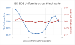
SiO2 Uniformity
Measured in June 2010 (Demis D. John)
| Thickness (nm) | Refractive Index
(at 632nm) | |
|---|---|---|
| Mean (Avg.), nm | 1677.80 | 1.480 |
| Min | 1671.09 | 1.479 |
| Max | 1688.9 | 1.482 |
| Std. Deviation (nm) | 5.99 | 8.6e-4 |

Si3N4 deposition (IBD)
- Si3N4 [IBD] Standard Recipe - "1_Si3N4_Dep"
- Si3N4 [IBD] Process Control Data
Si3N4 Thin-Film Properties (IBD)
- Deposition Rate: ≈ 4.10 nm/min (users must calibrate this prior to critical deps)
- HF Etch Rate: ~11nm/min
- Stress ≈ -1590MPa (compressive)
- Refractive Index: ≈ 1.969
- Cauchy Parameters (350-2000nm):
- A = 2.000
- B = 0.01974
- C = 1.2478e-4
Ta2O5 deposition (IBD)
- Ta2O5 [IBD] Standard Recipe - "1_Ta2O5_dep"
- Ta2O5 [IBD] Process Control Data
- Ta2O5 [IBD] Historical Data - before Oct. 2021
Ta2O5 Thin-Film Properies (IBD)
- Ta2O5 1hr depositions:
- Deposition Rate: ≈ 7.8 nm/min (users must calibrate this prior to critical deps)
- HF Etch Rate ≈ 2 nm/min
- Stress ≈ -232MPa (compressive)
- Refractive Index: ≈ 2.172
- Cauchy Parameters (350-2000nm):
- A = 2.1123
- B = 0.018901
- C = -0.016222
Al2O3 deposition (IBD)
- Al2O3 [IBD] Standard Recipe - "1_Al2O3_dep"
- Al2O3 [IBD] Process Control Data
Al2O3 Thin-Film Properties (IBD)
- Deposition Rate ≈ 2.05nm/min (users must calibrate this prior to critical deps)
- HF etch rate ≈ 167nm/min
- Stress ≈ -332MPa (compressive)
- Refractive Index: ≈ 1.656
- Cauchy Parameters (350-2000nm):
- A = To Be Added
- B =
- C =
- Absorbing < ~350nm
TiO2 deposition (IBD)
- TiO2 [IBD] Standard Recipe - "1_TiO2_dep"
- TiO2 [IBD] Process Control Data
TiO2 Thin-Film Properties (IBD)
- Deposition Rate: ≈ 1.29 nm/min (users must calibrate this prior to critical deps)
- HF etch rate ~5.34nm/min
- Stress ≈ -445MPa (compressive)
- Refractive Index: ≈ 2.259
- Cauchy Parameters (350-2000nm):
- A = 2.435
- B = -4.9045e-4
- C = 0.01309
- Absorbing < ~350nm wavelength
SiOxNy deposition (IBD)
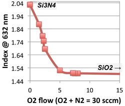
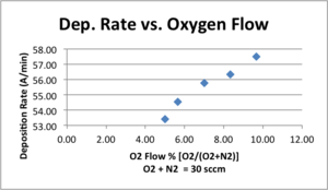
These are some old (2010), initial characterizations only. A recipe improvement would be to increase the Assist O2+N2 = 60sccm total, increasing repeatability by getting away from the low-flow limit of the MFC's. Data provided by Demis D. John, 2010.
 |
 |
|---|
Standard Cleaning Procedure (IBD)
You must edit the "#_GridClean"("#" is your group number) steps in your Process according to the following times:
- 5min GridClean for 1hr or less deposition
- 10min GridClean for up to 2hrs of dep.
- Do not deposit for longer than 2hrs - instead break up your Process into multiple 2-hr subroutines with cleans in between. See the recipe "1_SiO2_Dep_Multi" for an example.
Standard Grid-Clean Recipe
Reference Recipes (Disabled Tools)
Sputter 2 (SFI Endeavor)
This Tool has been Disabled, and is not available for use any more! These recipes are displayed here for historical/reference purposes only.
Al Deposition (Sputter 2)
AlNx Deposition (Sputter 2)
Au Deposition (Sputter 2)
TiO2 Deposition (Sputter 2)