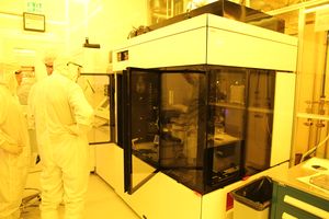
Stepper 2 (AutoStep 200)
| ||||||||||||||||||||||||||||||
About
Our GCA wafer stepper is an i-line (365 nm) step and repeat exposure tool for doing lithography that requires high resolution (≥500nm) and/or critical alignment (≥150nm).
The system has been modified to accept piece parts (down to smaller than 10mm x 10mm) up to 6” diameter wafers using manual wafer loading. The maximum square die size is 14.8 mm x 14.8 mm.
The system has an Olympus 2145 (N.A. = 0.45) lens that reduces the mask image by 5x and gives an ultimate resolution of better than 0.5 um in the center of the lens field. The system can easily produce 0.7 um isolated lines across the entire field. The Autostep200 system has 3-point wafer leveling to improve focus uniformity across the field. Autofocus is used to determine the sample surface relative to the lens, making the focus stable and repeatable for different thickness of wafer. The stages are controlled by stepper motors and laser interferometers.
Using the "global", manual alignment, better than 0.25 um alignment error is achievable. Using the DFAS "local" alignment system, alignment error better than 0.15 um is achieved. With the 1000 W Hg arc lamp, we get about 420 mW/cm² of i-line intensity at the wafer.
The system is computer controlled with the capability to program and save a wide variety of exposure jobs. We also have unlimited phone support for system problems through a service contract.
Tutorial: If you are not familiar with the differences between Contact Litho and Stepper Litho, please review this short tutorial: Demis D. John - Stepper_Reticle_Layout_vs_Wafer_Layout.pdf
Detailed Specifications
- Lens: Olympus 2145: NA = 0.45; Depth of field = 1.2 um for 0.6 um process
- Maximum die size: ~ 15 mm x 15 mm
- Maximum substrate thickness: we have various chucks with shims to allow different thicknesses - contact staff for info.
- Resolution: 400-450 nm for R&D; 700 nm over entire 15 mm x 15 mm field
- Registration tolerance: 0.25 µm global alignment; Max 0.15 µm local alignment (with care, you can achieve < 0.10 µm registration)
- Substrate size: ~ 10 x 10 mm up to 100 mm (150 mm possible, we don't provide the vacuum chuck for it).
- Computer programmable, recipes saved on hard disk
- Reticle alignment fiducials and global/local fiducials available - contact us for CAD files.
Process Information
Photomask Info
- Autostep 200 Mask Making Guidance - information on designing and ordering your photomasks for this system.
Recipes
Photoresists
- The laboratory contains a variety of i-line compatible photoresists. See the Photolith. Recipes Page for detailed processing info (bakes/spins/exposure does etc.). Basic photoresists include:
- 955CM-0.9 for 0.7-1.0 um thick positive processes.
- AZ5214E for 1.0 um thick image reversal (negative) process.
- SPR955CM-1.8 for 1.5-2.0 um thick positive processes.
- SPR220-3 for 2.5-5 um thick positive process.
- SPR220-7 for >5 um thick positive processes.
- AZnLOF5510 for <1.0um and AZnLOF 2020 for 1.5-3 um negative resist process.
- Shipley LOL-2000 is also used as an underlayer for high resolution lift-off processes.
CAD Files
- Photomask Template: Dark-field (polygons/objects are clear) at 5x Magnification (GDS)
- This template is designed to be submitted to the photomask vendor to print as-is, no scaling applied.
- Insert your designs into the template as Instances scaled UP by 5x.
- Global Alignment Mark CAD File (GDS)
- Local Alignment Mark CAD File (GDS)
- Local Alignment Mark CAD File: Dotted (GDS)
- This dotted version works for low-contrast layers (eg. mark etched into very thin ≤100nm layer).
- See the Calculators + Utilities > CAD Files & Templates page for other useful CAD files, such as overlay verniers, vented fonts etc.
Service Provider
- 3C Technical - The company that services the stepper.
Operating Procedures
Tool Operation
- Running the JOB - One Page Instructions
- Standard Operating Procedure
- Optimizing the Process
- Troubleshooting and Recovery
Job Programming
- Programming a Job - Detailed instructions
- Programming Differences between Piece-parts and Full Wafers
Reference/Other Info
- Mask Making Guidelines - for designing and ordering photomasks
- Focus Mechanism & Manual Focus - Info on how the focus system works and how to use Manual Focus effectively. Written by Molly Piels.
- User Accessible Commands
- Training Manual (old version)
Maintenance Procedures
These procedures are for Staff / Special use only - contact staff if you think you need to run these!
