Stepper Mask-Making Guidelines (Generic)
Generic Stepper Mask Parameters
Tutorial: If you are not familiar with the difference between designing Contact Litho Masks and Stepper Litho Masks/Reticles, please review this short tutorial:
- Demis D. John - Stepper Reticle Layout vs. Wafer Layout.pdf
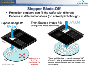
Click for TutorialReticle Patterns (“images”) are independent of wafer-layout. The reticle could contain 20 variations while the wafer could have only a few of the Images actually exposed, in any desired location on the wafer, determined by the Job Programming.
For the stepper you are designing for, make sure you know:
- Magnification: Our I-Line steppers are 5x, and the DUV stepper is 4x reduction.
- Maximum exposure field size:
- Your designs must fit within this area, including spacing between adjacent Image Fields.
- GCA AutoStep200 & GCA 6300
- 14.8 x 14.8 mm at 1x wafer-scale (74mm square at 5x reticle-scale)
- ASML PAS5500/300 (DUV):
- Intersection of a 21x25mm rectangle and an approx. 31mm circle:
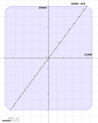
ASML mask design area - intersection of 21x25mm rectangle and 31mm circle, a rectangle with the corners cutoff.
- A common design area is: 21x21mm or 22x22mm (closer to edges)
- 21x25mm, but 800µm on the corners will get cut off.
- Intersection of a 21x25mm rectangle and an approx. 31mm circle:
- Minimum gap between adjacent patterns/images that must be dark chrome (for the system's reticle shutters to block adjacent images)
- GCA AutoStep 200: ≥1mm @ 1x wafer-scale (≥5mm @ 5x mask-scale) of chrome
- ASML PAS 5500/300 (DUV): ≥1mm of Chrome at 1x wafer-scale
- Either the quoted product number from our photomask vendor quotes, or reticle size/thickness/material
- For the GCA Steppers: 5x5x0.090 inches, soda-lime glass, 5x magnification/reduction
- For the ASML PAS 5500/300: 6x6x0.250 inches, quartz, 4x magnification/reduction
- Academic users only: contact Demis for our mask plate quotes. Industrial users must contact photomask vendors themselves to get their own quotes. One of the following:
- "GCA AutoStep 200" - this works for the GCA 6300 as well
- "ASML PAS 5500/330" - this is for the 248nm DUV Stepper.
- System model number - ask the photomask vendor to Magnify and Insert your 1x wafer-scale designs into the appropriate stepper template for the model of Stepper you are using.

These values will vary depending on the stepper you're designing for. Contact the Stepper's Process Expert or Tool Supervisor to find out/confirm the values on your mask order form.
Definitions for Mask/Reticle Order Form
When submitting the photo mask order, the following notes & definitions apply:
- "Grade" or "Product Code" will be one of the items on our quote. This will specify the glass type (soda-lime or quartz), plate size (4" square and 0.090" thick, for example), and the resolution. The grade choice determines the price, and is chosen based on required feature size (smaller feature size is more expensive). This is found on the vendor's quote, or you ask the vendor for a price based on desired minimum feature size (smallest feature actually present on your CAD file).
- Although you will submit your CAD file at 1x wafer scale, the actual reticle is printer larger by the stepper's magnification (eg. 4x or 5x mag, depending on the stepper system), so make sure to choose your reticle grade accounting for this; eg. If my CAD has 1.0µm lines smallest feature, I should choose a photomask grade better/equal to 4.0µm for a stepper with 4x reduction.
- "Address Unit" - this is the "pixel size" or "raster scan step" for the mask write. The smaller the address unit, the longer the mask write time, so the higher the cost. Also the vendor may need to use a more expensive writer for smaller Address Units. Typically 50nm (cheap/coarse) down to 1nm (expensive/precise).
- “GDS Level” is the “layer number”.
- "topcell" or "structure name": which Cell in your CAD file contains the hierarchy of patterns to print.
- Mirroring should be "Right-Reading (ie. legible text) when viewed with Chrome Down", if your CAD is exactly what you want on the wafer, for all our systems.
- If you are doing backside alignment, make sure you Mirror your layers appropriately! We usually perform the mirroring ourselves in CAD and still submit the order with "Right Reading/Chrome Down", to avoid any confusion.
- Polarity is usually "Polygons are Clear/Dark Field", to ensure the regions between Images (patterns) and outer portions are all opaque Chrome. However, you can make your mask Polygons are Dark/Clear Field, you just need to add polygons to put Chrome in between your adjacent Images. (FYI, "Digitized data" is another way of saying "The polygons you drew".)
- Whether you are planning to use Positive or Negative photoresist makes a difference! Plan your process and the Mask Polarity accordingly.
- “Min. Feature on Mask” refers to minimum clear or opaque feature, assuming features similar to lines/spaces. This should be at the reticle-scale since that is what the Photomask company will be making & fabricating for you - see "Grade" above.
- “Min. Contact” refers to features with aspect ratio close to 1:1, eg. Squares and circles (such as "contact pads"). These have a separate spec (often worse) due to the mask manufacturing process, so make sure to choose the appropriate grade of photomask with this in mind.
- “CD”, or "Critical Dimension" - Choose a CD similar to your most critical feature (scaled to the 5x/4x reticle scale), so the photomask vendor will print & measure & guarantee test structures at that exact size. They'll usually write a small CD pattern somewhere on the edge of the plate, and will guarantee that CD size. Should not be smaller than the Min. Feature size chosen, or they'll require you to choose a more expensive grade to achieve that smaller size..
- "Registration" - we usually choose "Not needed" for our plates. This refers to whether the patterns needs to be accurately aligned to the glass plate itself - which is not a problem for Stepper masks since the system aligns to the written Chrome patterns only.
CAD Tips
- Design with (0,0) the origin at the Center of your mask plate, and/or wafer-center.
- See here for enabling the Origin (0,0) marker on KLayout.
- By default, Wafer flat is Down (–Y) with respect to your CAD file for most systems.
- Utilize the "Cell" and "Cell Instancing" functionality in your CAD layout program! (aka. a "Block" in AutoCAD). Highly recommended to use KLayout, not AutoCAD. See Calculators + Utilities > CAD Design Tips for tutorials.
- Center your entire design around the coordinates (0,0). (0,0) should always be the center of your device, wafer and/or photomask/reticle Cells. Photomask vendors should then NOT "auto center" your designs on the plate.
- Inside each sub-Cell, also design around the cell's (0,0) origin.
- Create a Cell called "reticle_layout" or similar, that is an exact representation of what the printed reticle patterns should look like (typically at 1x wafer-scale, if not including the outer templates for the stepper system). Instance the Device's Cells into reticle_layout, and reference this Cell on your mask order form. (You can also Instance the same cells into "device_layout" and "wafer_layout" cells during design/verification.).
- You don't have to include the Stepper outer template - usually photomask vendors can add the reticle-level alignment marks, barcodes etc.; you just send them your 1x wafer-level designs, and instruct the vendor to magnify by 5x/4x, insert into a template for the specified stepper (tell them the model), and they can do the rest.
- For our GCA systems, which we have the full reticle template files for, you can optionally do the 5x magnification and insert into the template file yourself if desired.
If you follow the above rules, your printed "reticle_layout" Cell will have Instances of each of your design's Images/patterns, and the coordinates/sizes of these Cells are exactly what you use to write your Stepper program.
See the example CAD Files here:
Generic Stepper design/programming CAD files & spreadsheets
- Example Toppan Order Form via Digidat
- Academic users may request the UCSB Nanofab's quotes from various photomask vendors.
- Fill out this Spreadsheet before programming your job on the machine, using your CAD file:
- UCSB_Stepper_-_Programming_Worksheet.pptx - New version of the spreadsheet below, that also includes the wafer-layout info needed to generate a basic stepper exposure program.
- Stepper Reticle Programming Params - MASKJAN2020 v1.xlsx (example for fictional barcode "MASKJAN2020") - Spreadsheet form of the above PPT. Faster to fill out for "expert" stepper users.
- On-wafer alignment marks:
- Please check for the specific Stepper you are using.
- This pattern is usually available on a system reticle - you are not required to include the alignment mark pattern in your own designs, but you may do so if desired.
- Ask the tool supervisor for the CAD file for alignment marks if needed.
Example CAD File and Programming
Using an Example CAD file, here is the corresponding Mask Order Form & Spreadsheet:
- Example CAD file from Utilities > CAD Layout > Example CAD File, designed in KLayout.
- Example "Stepper Reticle Programming Params" spreadsheet for reticle "DEM-2020-03"
- Example Reticle Order Form for reticle "DEM-2020-03"