Stepper 2 (AutoStep 200): Difference between revisions
(→About) |
(link to FEM analysis pages, Stepper 2 recipes page) |
||
| (93 intermediate revisions by 8 users not shown) | |||
| Line 1: | Line 1: | ||
{{ |
{{tool2_DJ|{{PAGENAME}} |
||
|picture=Stepper2.jpg |
|picture=Stepper2.jpg |
||
|type = Lithography |
|type = Lithography |
||
|super= |
|super= Biljana Stamenic |
||
|super2 = Bill Millerski |
|||
|phone=(805)839-3918x213 |
|||
|location=Bay 6 |
|location=Bay 6 |
||
|email=abrahamsen@ece.ucsb.edu |
|||
|description = GCA 200 I-Line Wafer Stepper |
|description = GCA 200 I-Line Wafer Stepper |
||
|manufacturer = GCA |
|manufacturer = GCA |
||
|materials = |
|materials = |
||
|recipe = Lithography |
|||
|toolid=38 |
|toolid=38 |
||
}} |
}} |
||
= |
==About== |
||
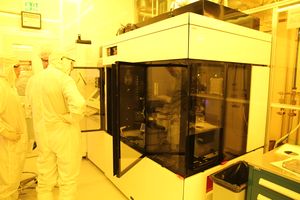
Our GCA wafer stepper is an i-line (365 nm) step and repeat exposure tool for doing lithography that requires high resolution (≥500nm) and/or critical alignment (≥150nm). |
|||
Our GCA wafer stepper is an i-line (365 nm) step and repeat exposure tool for doing lithography that requires high resolution and/or critical alignment. The system has been modified to accept piece parts (down to ~15 mm x 15 mm) up to 6” diameter wafers using manual wafer loading. The maximum die size is ~ 15 mm x 15 mm. The system has an Olympus 2142 (N.A. = 0.42) lens that reduces the mask image by 5 x and gives an ultimate resolution of ~ 0.5 um in the center of the lens field. The system can easily produce 0.7 um isolated lines across the entire field. Autofocus is used to determine the sample surface relative to the lens, making the focus stable and repeatable for different thickness of wafer. The stages are controlled by stepper motors and laser interferometers. Using the global, manual alignment, better than 0.25 um alignment error is achievable. Using the DFAS local alignment system, alignment error better than 0.15 um is achieved. With the 350 W Hg arc lamp, we get about 180 W/cm² of i-line intensity at the wafer. |
|||
The system has been modified to accept piece parts (down to smaller than 10mm x 10mm) up to 6” diameter wafers using manual wafer loading. The maximum square die size is 14.8 mm x 14.8 mm. |
|||
The system is computer controlled with the capability to program and save a wide variety of exposure jobs. We also have unlimited phone support for system problems through a service contract. The laboratory contains a variety of i-line compatible photoresists. SPR510A, 955CM, 950-0.8 for 0.7-1.0 um thick positive processes. AZ5214E for 1.0 um thick image reversal (negative) process. SPR955CM-1.8 for 1.5-2.0 um thick positive processes. SPR220-3 for 2.5-5 um thick positive process. SPR220-7 and AZ9260 for >5 um thick positive processes. AZnLOF5510 for <1.0um and AZnLOF 2020 for 1.5-3 um negative resist process. Shipley LOL-2000 is also used as an underlayer for high resolution lift-off processes. |
|||
The system has an Olympus 2145 (N.A. = 0.45) lens that reduces the mask image by 5x and gives an ultimate resolution of better than 0.5 um in the center of the lens field. The system can easily produce 0.7 um isolated lines across the entire field. The Autostep200 system has 3-point wafer leveling to improve focus uniformity across the field. Autofocus is used to determine the sample surface relative to the lens, making the focus stable and repeatable for different thickness of wafer. The stages are controlled by stepper motors and laser interferometers. |
|||
=Detailed Specifications= |
|||
*Lens: Olympus 2145: NA = 0.45; Depth of field = 1.2 mm for 0.6 um process |
|||
Using the "global", manual alignment, better than 0.25 um alignment error is achievable. Using the DFAS "local" alignment system, alignment error better than 0.15 um is achieved. With the 1000 W Hg arc lamp, we get about 420 mW/cm² of i-line intensity at the wafer. |
|||
The system is computer controlled with the capability to program and save a wide variety of exposure jobs. We also have unlimited phone support for system problems through a service contract. |
|||
'''Tutorial:''' If you are not familiar with the differences between Contact Litho and Stepper Litho, please review this short tutorial: [https://wiki.nanofab.ucsb.edu/w/images/c/cb/Demis_D_John_-_Stepper_Reticle_Layout_vs_Wafer_Layout.pdf Demis D. John - Stepper_Reticle_Layout_vs_Wafer_Layout.pdf] |
|||
==Detailed Specifications== |
|||
*Lens: Olympus 2145: NA = 0.45; Depth of field = 1.2 um for 0.6 um process |
|||
*Maximum die size: ~ 15 mm x 15 mm |
*Maximum die size: ~ 15 mm x 15 mm |
||
*Maximum substrate thickness: we have various chucks with shims to allow different thicknesses - contact staff for info. |
|||
*Resolution: 350-400 nm for R&D; 500 nm over entire 15 mm x 15 mm field |
|||
*Resolution: 400-450 nm for R&D; 700 nm over entire 15 mm x 15 mm field |
|||
*Registration tolerance: 0.30 mm global alignment; Max 0.15 mm local alignment (with care, you can achieve < 0.10 mm registration) |
|||
*Registration tolerance: 0.25 µm global alignment; Max 0.15 µm local alignment (with care, you can achieve < 0.10 µm registration) |
|||
*Minimum substrate size: ~ 10 x 10 mm |
|||
*Substrate size: ~ 10 x 10 mm up to 100 mm (150 mm possible, we don't provide the vacuum chuck for it). |
|||
*Computer programmable, recipes saved on hard disk |
*Computer programmable, recipes saved on hard disk |
||
*Reticle alignment fiducials and global/local fiducials available |
*Reticle alignment fiducials and global/local fiducials available - contact us for CAD files. |
||
*Mask Plates: 5x5x0.090 inches, 5x reduction, typically Soda Lime Glass (Quartz is also acceptable), no pellicle. |
|||
==Process Information== |
|||
===Photomask Info=== |
|||
*[[Autostep 200 Mask Making Guidance]] - ''information on designing and ordering your photomasks for this system.'' |
|||
===Recipes=== |
|||
*[https://wiki.nanofab.ucsb.edu/wiki/Stepper_Recipes#Stepper_2_.28AutoStep_200.29 Photolitography Recipes]* |
|||
===Photoresists=== |
|||
*The laboratory contains a variety of i-line compatible photoresists. See the [https://signupmonkey.ece.ucsb.edu/w/index.php?title=Lithography_Recipes#Photolithography_Recipes Photolith. Recipes Page] for detailed processing info (bakes/spins/exposure does etc.). Basic photoresists include: |
|||
**955CM-0.9 for 0.7-1.0 um thick positive processes. |
|||
**AZ5214E for 1.0 um thick image reversal (negative) process. |
|||
**SPR955CM-1.8 for 1.5-2.0 um thick positive processes. |
|||
**SPR220-3 for 2.5-5 um thick positive process. |
|||
**SPR220-7 for >5 um thick positive processes. |
|||
**AZnLOF5510 for <1.0um and AZnLOF 2020 for 1.5-3 um negative resist process. |
|||
**Shipley LOL-2000 is also used as an underlayer for high resolution lift-off processes. |
|||
===CAD Files=== |
|||
*[[Media:GCA Stepper MaskPlate Master-DarkField 5x.gds|Photomask Template: Dark-field (polygons/objects are clear) at 5x Magnification (GDS)]] |
|||
**''This template is designed to be submitted to the photomask vendor to print as-is, no scaling applied.'' |
|||
**''Insert your designs into the template as Instances scaled UP by 5x.'' |
|||
*[[Media:GCA Global Mark.gds|Global Alignment Mark CAD File (GDS)]] |
|||
*[[Media:GCA Local Alignment Mark.gds|Local Alignment Mark CAD File (GDS)]] |
|||
*[[Media:GCA Local Alignment Mark Dotted.gds|Local Alignment Mark CAD File: Dotted (GDS)]] |
|||
**''This dotted version works for low-contrast layers (eg. mark etched into very thin ≤100nm layer).'' |
|||
*See the [[Calculators + Utilities#CAD%20Files%20.26%20Templates|Calculators + Utilities > CAD Files & Templates]] page for other useful CAD files, such as overlay verniers, vented fonts etc. |
|||
==Service Provider== |
|||
*[http://3ctechnical.com/index.html 3C Technical] - The company that services the stepper. |
|||
==Operating Procedures== |
|||
===Tool Operation=== |
|||
*[https://wiki.nanofab.ucsb.edu/w/images/0/05/Running_the_JOB-_One_Page_Instructions.pdf Running the JOB - One Page Instructions] |
|||
*[https://wiki.nanofab.ucsb.edu/w/images/f/f3/Autostep_200_-_Standard_Operating_Procedure-2023.pdf Standard Operating Procedure] |
|||
*[https://wiki.nanofab.ucsb.edu/w/images/3/39/Focus_and_exposure_optimization-_Autostep200-II.pdf Optimizing the Process] - Focus-Exposure Matrix (FEM) instructions |
|||
*[[Autostep 200 Troubleshooting and Recovery|Troubleshooting and Recovery]] |
|||
===Job Programming=== |
|||
*[https://wiki.nanofab.ucsb.edu/w/images/2/27/Autostep_200_-_Setting_up_the_Job.pdf Programming a Job] - Detailed instructions |
|||
*[[Stepper 2 (Autostep 200) - Job Programming|Programming Differences between Piece-parts and Full Wafers]] |
|||
===Video Training=== |
|||
These video trainings have bookmarks to skip to specific sections - use them as reference. |
|||
Remember, you are NOT authorized to use the system until a [[Biljana Stamenic|supervisor]] grants you access. |
|||
{| class="wikitable" |
|||
| colspan="2" |To view the vids: after clicking the above link, do the following |
|||
|- |
|||
|(1) Choose "Canvas" from the dropdown |
|||
[[File:2024-01 PanOpto - Canvas dropdown.png|alt=screenshot of Canvas dropdown|270x270px]] |
|||
and then:<br /> |
|||
|(2) click "UCSB Users" and |
|||
login with your '''UCSB NetID'''. |
|||
[[File:2024-01 PanOpto - UCSB Login.png|alt=screenshto of UCSB Users button|203x203px]] |
|||
|} |
|||
*[https://gauchocast.hosted.panopto.com/Panopto/Pages/Viewer.aspx?id=fa7462ce-6f71-49b4-89c4-b20201393f94 '''Video Training for the GCA AutoStep 200'''] on Canvas/PanOpto. |
|||
::[[File:GCA Autostep 200 training vid title screen.png|none|thumb|300x300px|link=https://gauchocast.hosted.panopto.com/Panopto/Pages/Viewer.aspx?id=fa7462ce-6f71-49b4-89c4-b20201393f94]] |
|||
===Reference/Other Info=== |
|||
*[[Autostep 200 Mask Making Guidance|'''Mask Making Guidelines''']] - ''for designing and ordering photomasks'' |
|||
*[https://wiki.nanofab.ucsb.edu/w/images/2/2e/Autostep_200_Stepper_manual_focus.pdf Focus Mechanism & Manual Focus] - Info on how the focus system works and how to use Manual Focus effectively. Written by Molly Piels. |
|||
*[https://wiki.nanofab.ucsb.edu/w/images/e/e1/AUTOSTEP_200_User_Accessible_Commands_010524.pdf User Accessible Commands] |
|||
*[https://wiki.nanofab.ucsb.edu/w/images/5/54/Autostep200_Training_Old_Training_Manual.pdf Training Manual (old version)] |
|||
== Recipes == |
|||
* '''[[Stepper Recipes#Stepper 2 (AutoStep 200)|Recipes > Lithography > Stepper Recipes > Stepper #2]]''' - starting processes for various I-Line photoresists, including Dose/Focus values.To calibrate your own Litho processes, you will need to: |
|||
* Run your own [https://wiki.nanofab.ucsb.edu/w/images/3/39/Focus_and_exposure_optimization-_Autostep200-II.pdf Focus Exposure Matrix] - instructions for doing this on the AutoStep 200. |
|||
* [[Lithography Calibration - Analyzing a Focus-Exposure Matrix]] - how to analyze an FEM |
|||
Litho. recipes for all our photolith. tools can be found on the [[Lithography Recipes#Photolithography%20Recipes|Photolithography Recipes]] page. |
|||
==Maintenance Procedures== |
|||
''These procedures are for Staff / Special use only - contact staff if you think you need to run these!'' |
|||
*[https://wiki.nanotech.ucsb.edu/w/images/5/5e/Autostep_200_Restart_SOP_June_2021.pdf Shutdown + Startup Procedure] |
|||
==Related Tools== |
|||
=See Also= |
|||
* [http://3ctechnical.com/index.html 3C Technical] - The company that services the stepper. |
|||
*[[Stepper 1 (GCA 6300)]] - similar tool, compatible photomasks, but with manual photomask alignment and no DFAS. Can't shoot multiple mask plates in single session. |
|||
=Documentation= |
|||
* [[media:GCA-200-Training-Manual.pdf|Training Manual]] |
|||
Latest revision as of 19:30, 26 October 2024
| ||||||||||||||||||||||||||||||
About
Our GCA wafer stepper is an i-line (365 nm) step and repeat exposure tool for doing lithography that requires high resolution (≥500nm) and/or critical alignment (≥150nm).
The system has been modified to accept piece parts (down to smaller than 10mm x 10mm) up to 6” diameter wafers using manual wafer loading. The maximum square die size is 14.8 mm x 14.8 mm.
The system has an Olympus 2145 (N.A. = 0.45) lens that reduces the mask image by 5x and gives an ultimate resolution of better than 0.5 um in the center of the lens field. The system can easily produce 0.7 um isolated lines across the entire field. The Autostep200 system has 3-point wafer leveling to improve focus uniformity across the field. Autofocus is used to determine the sample surface relative to the lens, making the focus stable and repeatable for different thickness of wafer. The stages are controlled by stepper motors and laser interferometers.
Using the "global", manual alignment, better than 0.25 um alignment error is achievable. Using the DFAS "local" alignment system, alignment error better than 0.15 um is achieved. With the 1000 W Hg arc lamp, we get about 420 mW/cm² of i-line intensity at the wafer.
The system is computer controlled with the capability to program and save a wide variety of exposure jobs. We also have unlimited phone support for system problems through a service contract.
Tutorial: If you are not familiar with the differences between Contact Litho and Stepper Litho, please review this short tutorial: Demis D. John - Stepper_Reticle_Layout_vs_Wafer_Layout.pdf
Detailed Specifications
- Lens: Olympus 2145: NA = 0.45; Depth of field = 1.2 um for 0.6 um process
- Maximum die size: ~ 15 mm x 15 mm
- Maximum substrate thickness: we have various chucks with shims to allow different thicknesses - contact staff for info.
- Resolution: 400-450 nm for R&D; 700 nm over entire 15 mm x 15 mm field
- Registration tolerance: 0.25 µm global alignment; Max 0.15 µm local alignment (with care, you can achieve < 0.10 µm registration)
- Substrate size: ~ 10 x 10 mm up to 100 mm (150 mm possible, we don't provide the vacuum chuck for it).
- Computer programmable, recipes saved on hard disk
- Reticle alignment fiducials and global/local fiducials available - contact us for CAD files.
- Mask Plates: 5x5x0.090 inches, 5x reduction, typically Soda Lime Glass (Quartz is also acceptable), no pellicle.
Process Information
Photomask Info
- Autostep 200 Mask Making Guidance - information on designing and ordering your photomasks for this system.
Recipes
Photoresists
- The laboratory contains a variety of i-line compatible photoresists. See the Photolith. Recipes Page for detailed processing info (bakes/spins/exposure does etc.). Basic photoresists include:
- 955CM-0.9 for 0.7-1.0 um thick positive processes.
- AZ5214E for 1.0 um thick image reversal (negative) process.
- SPR955CM-1.8 for 1.5-2.0 um thick positive processes.
- SPR220-3 for 2.5-5 um thick positive process.
- SPR220-7 for >5 um thick positive processes.
- AZnLOF5510 for <1.0um and AZnLOF 2020 for 1.5-3 um negative resist process.
- Shipley LOL-2000 is also used as an underlayer for high resolution lift-off processes.
CAD Files
- Photomask Template: Dark-field (polygons/objects are clear) at 5x Magnification (GDS)
- This template is designed to be submitted to the photomask vendor to print as-is, no scaling applied.
- Insert your designs into the template as Instances scaled UP by 5x.
- Global Alignment Mark CAD File (GDS)
- Local Alignment Mark CAD File (GDS)
- Local Alignment Mark CAD File: Dotted (GDS)
- This dotted version works for low-contrast layers (eg. mark etched into very thin ≤100nm layer).
- See the Calculators + Utilities > CAD Files & Templates page for other useful CAD files, such as overlay verniers, vented fonts etc.
Service Provider
- 3C Technical - The company that services the stepper.
Operating Procedures
Tool Operation
- Running the JOB - One Page Instructions
- Standard Operating Procedure
- Optimizing the Process - Focus-Exposure Matrix (FEM) instructions
- Troubleshooting and Recovery
Job Programming
- Programming a Job - Detailed instructions
- Programming Differences between Piece-parts and Full Wafers
Video Training
These video trainings have bookmarks to skip to specific sections - use them as reference.
Remember, you are NOT authorized to use the system until a supervisor grants you access.
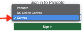
| To view the vids: after clicking the above link, do the following | |
| (1) Choose "Canvas" from the dropdown
and then: |
(2) click "UCSB Users" and
login with your UCSB NetID. |
- Video Training for the GCA AutoStep 200 on Canvas/PanOpto.
Reference/Other Info
- Mask Making Guidelines - for designing and ordering photomasks
- Focus Mechanism & Manual Focus - Info on how the focus system works and how to use Manual Focus effectively. Written by Molly Piels.
- User Accessible Commands
- Training Manual (old version)
Recipes
- Recipes > Lithography > Stepper Recipes > Stepper #2 - starting processes for various I-Line photoresists, including Dose/Focus values.To calibrate your own Litho processes, you will need to:
- Run your own Focus Exposure Matrix - instructions for doing this on the AutoStep 200.
- Lithography Calibration - Analyzing a Focus-Exposure Matrix - how to analyze an FEM
Litho. recipes for all our photolith. tools can be found on the Photolithography Recipes page.
Maintenance Procedures
These procedures are for Staff / Special use only - contact staff if you think you need to run these!
Related Tools
- Stepper 1 (GCA 6300) - similar tool, compatible photomasks, but with manual photomask alignment and no DFAS. Can't shoot multiple mask plates in single session.


