Stepper 3 (ASML DUV): Difference between revisions
moved UCSB Test reticles to "Design & Fabrication Tools" section |
No edit summary |
||
| (104 intermediate revisions by 3 users not shown) | |||
| Line 1: | Line 1: | ||
{{ |
{{tool2|{{PAGENAME}} |
||
|picture=ASML.jpg |
|picture=ASML.jpg |
||
|type = Lithography |
|type = Lithography |
||
|super= Demis D. John |
|super= Demis D. John |
||
|super2= Bill Millerski |
|||
|location=Bay 7 |
|location=Bay 7 |
||
|description = |
|description = Deep-UV Stepper Photolithography |
||
|model = PAS 5500/300 |
|||
|manufacturer = [http://www.asml.com ASML] |
|manufacturer = [http://www.asml.com ASML] |
||
|ToolType = Lithography |
|ToolType = Lithography |
||
| Line 11: | Line 13: | ||
|toolid=51 |
|toolid=51 |
||
}} |
}} |
||
{{ToolActions |
|||
|toolid = 51 |
|||
|ProcessControlURL = Stepper_3_(ASML_DUV)#Process_Control_Data |
|||
|ProceduresURL = |
|||
|TrainingURL = Stepper_3_(ASML_DUV)#Training_Procedure |
|||
}} |
|||
=About= |
==About== |
||
===General Capabilities/Overview=== |
|||
The ASML 5500 stepper is a 248nm DUV stepper for imaging dense features down to below 200nm and isolated line structures down to below 150nm. Overlay accuracy is better than 30nm. |
|||
The ASML 5500 stepper is a 248nm (KrF) DUV stepper for imaging dense features down to below 200nm and isolated line structures down to below 150nm (with effort). 300nm+ features are relatively "easy" to resolve. Layer-to-layer overlay accuracy is better than 30nm. |
|||
The system is configured for 4” wafers |
The system is configured for 4” wafers. The system is designed for high throughput, so shooting multiple 4" wafers is extremely fast, typically minutes per wafer, but any size other than 4-inch is difficult to work with (see below for more info). Additionally, exposure jobs are highly programmable, allowing for very flexible exposures of multiple aligned patterns from multiple masks/reticles in a single session, allowing for process optimization of large vs. small features in a single lithography. |
||
The full field useable exposure area is limited to the intersection of a 31mm diameter circle and a rectangle of dimensions 22mm x 27mm. See the [[ |
The full field useable exposure area is limited to the intersection of a 31mm diameter circle and a rectangle of dimensions 22mm x 27mm. Users have stitched multiple photomasks together with success. See the [[Stepper 3 (ASML DUV)#Mask Design and CAD files|Mask Making Guidelines page]] for more info on exposure field sizes and how to order your mask plates. |
||
==== Stepper Tutorial ==== |
|||
Resists Used (see [https://www.nanotech.ucsb.edu/wiki/index.php/Lithography_Recipes#Photolithography_Recipes PhotoLith. Recipes] for full process info): |
|||
If you are not familiar with how Stepper Litho is different from our lithography methods, please review this short tutorial: |
|||
[https://wiki.nanofab.ucsb.edu/w/images/c/cb/Demis_D_John_-_Stepper_Reticle_Layout_vs_Wafer_Layout.pdf '''Stepper Reticle Layout vs Wafer Layout (Demis D. John)'''] - Explains the following: |
|||
* That a Stepper mask layout is very different than other litho systems. |
|||
* That a Stepper mask can have ''many'' designs, and flexibly pattern the wafer with combos of designs. |
|||
[[Stepper Reticle Layout (Advanced) - Complex Experiments and Variations|'''Stepper Reticle Layout (Advanced) - Complex Experiments and Variations''']] |
|||
* If you need many design variations on your wafer, this is an efficient way to utilize stepper reticles. |
|||
===Photoresists Available=== |
|||
''See [https://wiki.nanotech.ucsb.edu/w/index.php?title=Lithography_Recipes#Photolithography_Recipes PhotoLith. Recipes] for full process info & links to PR datasheets.'' |
|||
*UV210-0.3 - Positive: 300nm nominal thickness |
*UV210-0.3 - Positive: 300nm nominal thickness |
||
| Line 32: | Line 53: | ||
AZ300MIF Developer for all processes |
AZ300MIF Developer for all processes |
||
Many of these DUV PR's are also able to be exposed with [[E-Beam Lithography System (JEOL JBX-6300FS)|EBL]]. |
|||
=Process Information= |
|||
===Part Size Limits=== |
|||
*[https://www.nanotech.ucsb.edu/wiki/index.php/Lithography_Recipes#Photolithography_Recipes '''Process Recipes Page'''] '''> "Stepper 3"''' - ''Established recipes and corresponding linewidths, photoresists etc.'' |
|||
With staff support, mounted pieces down to 14mm in size can be exposed using a 4” wafer as a carrier. Flatness will typically be worse in this situation, so small <<500nm features will usually have bad uniformity across the mounted part due to focus variations. Edge bead on irregular pieces (eg. quarter-wafers/squares) will significantly reduce yield/uniformity. |
|||
Multi-layer Alignment on mounted parts is particularly difficult, requiring either semi-permanent mounting to the carrier (eg. BCB, SU8 etc.) or significant difficulty/effort to re-align the part to the carrier wafer on each lithography (≤100µm re-mounting accuracy needed). |
|||
At this time the maximum wafer size is 4” (100mm) wafers with SEMI standard wafer flat (not Notch). |
|||
===Service Provider=== |
|||
*[http://www.asml.com ASML] - ASML performs quarterly periodic maintenance and provides on-demand support. |
|||
==Process Information== |
|||
*[https://wiki.nanotech.ucsb.edu/w/index.php?title=Lithography_Recipes#Photolithography_Recipes '''Process Recipes Page'''] '''> "Stepper 3"''' - ''Established recipes and corresponding linewidths, photoresists etc.'' |
|||
*Sample size: 100 mm wafers with SEMI std. major flat |
*Sample size: 100 mm wafers with SEMI std. major flat |
||
**''Piece-parts process is possible but difficult - contact |
**''Piece-parts process is possible but difficult - contact supervisor for info'' |
||
*Alignment Accuracy: < 50 nm |
*Alignment Accuracy: < 50 nm |
||
*Minimum Feature Size: ≤150 nm isolated lines, ≤200 nm dense patterns |
*Minimum Feature Size: ≤150 nm isolated lines, ≤200 nm dense patterns |
||
**''To achieve ≤200nm features with high uniformity, we recommend wafers with total thickness variation (TTV) ≤5µm, and designing your CAD with a smaller Image Size for the high-res. feature''. |
|||
*Maximum Wafer Bow: approx. 100 µm. (4-inch diam.) |
|||
*Wafer Thickness: Minimum ≈ 200µm, Maximum ≈ 1.1 mm |
|||
**''Near this value, and the job may fail or lose the wafer inside the machine due to wafer vacuum error.'' |
|||
*Maximum Dose: ~100mJ |
|||
**''Non-chemically amplified EBL resists are not permissible due to this limit.'' |
|||
===Maximum Wafer Bow=== |
|||
=Operating Procedures= |
|||
Measured over 90mm on the [[Film Stress (Tencor Flexus)|Tencor Flexus]] |
|||
*'''Do not run wafers with bow values higher than the following values''', contact supervisor for advice if needed. |
|||
*[[ASML Stepper 3 Standard Operating Procedure|Standard Operating Procedures]] |
|||
*Silicon wafers (~550µm thick): 100 µm will likely fail. |
|||
**''Exposing wafers, loading reticles, focus/exposure matrix'' |
|||
*Sapphire (less pliable), ≥60µm bow will intermittently fail - DO NOT RUN |
|||
*[//www.nanotech.ucsb.edu/wiki/images/f/f7/ASML_Job_Set-Up_Guide_v2.pdf Job Programming - Full] |
|||
**This applies especially for GaN-on-Sapphire, which often have high wafer bow. |
|||
*[//www.nanotech.ucsb.edu/wiki/images/c/cd/ASML_Job_Set-Up_Guide_simple_v1.pdf Job Programming- Simplified -Full Wafers] |
|||
*''Near these values, and you may lose the wafer inside the machine due to wafer vacuum error - DO NOT RUN if unsure.'' |
|||
*''Substrate material and substrate thickness affect this limit - please contact [[Demis D. John|supervisor]] for advice.'' |
|||
*You can '''stress-compensate''' wafers to reduce the wafer bow, eg. by depositing on the back side of the wafer. If your wafer is concave down, then depositing a ''compressive'' film on the back will reduce its curvature. Coat the backside of the wafer with compressive PECVD SiO2 or [[Sputtering Recipes#Si3N4 deposition .28IBD.29|IBD SiN]], or other compressive films for concave-down bow. |
|||
==Operating Procedures== |
|||
===Troubleshooting and Recovery=== |
|||
'''All procedures are access-restricted only to authorized users with a <u>UCSB NetID (''YourNetID''@ucsb.edu)</u>, by vendor request. |
|||
Please contact [[Demis D. John|supervisor]] for access/training. |
|||
=== [https://drive.google.com/drive/folders/1U9-03qU2htQp_5x39LNq-mn5Q3vXXLDf?usp=drive_link <u>ASML Operating Procedures</u>] === |
|||
*[[ASML Stepper 3 Error Recovery, Troubleshooting and Calibration|Error Recovery, Troubleshooting and Calibration]] |
|||
* Access-restricted google drive folder of PAS 5500/300 operating procedures. |
|||
**''Common errors/System Warnings, Wafer Handler Reset, System Calibration Verification'' |
|||
=== [https://docs.google.com/document/d/1T6Bc7A6YjxFyxMR9n35CCsmtJVRQen3m371Vd_Q9dlY/edit?usp=drive_link <u>Troubleshooting & Error Recovery</u>] === |
|||
*[[ASML 5500: Recovering from an Error|ASML 5500: Recovering from an Error/Wafer Retrieval]] |
|||
* common issues and fixes (access-restricted) |
|||
**''How to abort the job and recover your wafer.'' |
|||
=== [[Stepper 3 (ASML DUV)#Calibrating your Lithography Process|<u>Calibrate Your Litho Process</u>]] === |
|||
===Software Options=== |
|||
See this section for the basics on how to do this: [[Stepper 3 (ASML DUV)#Calibrating your Lithography Process|Stepper 3 (ASML DUV) > Recipes > Calibrating your Lithography Process]] |
|||
=== [https://docs.google.com/document/d/17jPek8P_SF1qRADS09ApoDgUiB_v0NFJsIVpkL-Kdag/edit#heading=h.fmorc9eu8hfz <u>Stepper #3 Training/Reference Videos</u>] === |
|||
*[[ASML Stepper 3 - Shifted Measurement Scans (SMS)|Shifted Measurement Scans]] - better tilt/level measurements for edge-die. |
|||
* The above linked videos provide bookmarked quick-reference to various tool procedures & programming. |
|||
*[[ASML Stepper 3 - Compound Image Design (CIDS)|Compound Image Design]] - flexible Image Distribution: grouping of Images with shifts, duplicate instances of Images, |
|||
**''To access, you must log in with your UCSB NetID, formatted like'' <u>MyNetID''@ucsb.edu''</u> ''- this is a Google login!'' |
|||
*[[ASML Stepper 3 - Job Creator|Job Creator]] - create binary ASML job files from ASCII text files. Python scripting in progress. |
|||
**''Please contact the [[Demis D. John|tool supervisor]] if you need access.'' |
|||
**[[UCSB NetID Login Troubleshooting|'''''Trouble accessing?''''' ''Please click here for tips.'']] |
|||
**'''''You are NOT authorized''' to use this tool until a tool supervisor authorizes you!'' |
|||
===Training Procedure=== |
|||
==Design & Fabrication Tools== |
|||
To get access to this tool, please do the following: |
|||
#Email the [[Demis D. John|supervisor]] for access to the training materials. Please provide your <u>UCSB NetID</u>. |
|||
*[[ASML 5500 Mask Making Guidelines|ASML 5500 Mask Making Guidelines]] - All the info you need to design and order a reticle for this system. |
|||
#Study the [https://docs.google.com/document/d/17jPek8P_SF1qRADS09ApoDgUiB_v0NFJsIVpkL-Kdag/edit#heading=h.fmorc9eu8hfz training videos]. |
|||
*[[ASML Tools - Job Creator Python Module|ASML Job Creator]] - Python scripts for generating ASML Job Files. |
|||
##If you are a technician and will never program jobs, only Part 1 is necessary. |
|||
*[[ASML Stepper 3 - UCSB Test Reticles|UCSB Test Reticles]] - Alignment Markers, Resolution Testing etc. |
|||
#"Shadow" someone in your group who uses the machine, <u>until you are completely comfortable</u> with (1) wafer cleaning (critical), (2) reticle load/unload and (3) running a pre-made job. |
|||
#When you are ready, request a hands-on check-off on SignupMonkey by clicking this button:{{ToolTrainingButton|toolid=51}} |
|||
==Design Tools== |
|||
=Service Provider= |
|||
===Mask Design and CAD files=== |
|||
*[http://www.asml.com ASML] - ASML performs quarterly periodic maintenance and provides on-demand support. |
|||
*[https://wiki.nanofab.ucsb.edu/wiki/Stepper_Mask-Making_Guidelines_(Generic) '''Stepper Mask-Making Guidelines'''] - Info needed to design and order a reticle for our Stepper systems. This is minimal unrestricted info that is viewable without additional paperwork. |
|||
*'''[https://docs.google.com/document/d/1b9YT11RPsl-UlLvN74hrQvG01OcYDL16r6I5lPOlBEo/edit?usp=sharing ASML-specific Mask Making Guidelines (Private)]''' - More detailed info to design and order a reticle for this specific ASML system. |
|||
**''Access is restricted to trained users only by ASML's requirement - please contact [[Demis D. John|tool supervisor]] for access.'' |
|||
*'''Tutorial: [https://wiki.nanofab.ucsb.edu/w/images/c/cb/Demis_D_John_-_Stepper_Reticle_Layout_vs_Wafer_Layout.pdf Stepper Reticle Layout vs Wafer Layout (Demis D. John)]''' ''-'' explains how Stepper mask layout is very different than other litho systems. |
|||
*'''Tutorial: [[Stepper Reticle Layout (Advanced) - Complex Experiments and Variations]]''' - If you need many design variations on your wafer. |
|||
*See the [[Calculators + Utilities#CAD%20Files%20.26%20Templates|Calculators + Utilities > '''CAD Files & Templates''']] page for other useful CAD files, such as overlay verniers, vented fonts etc. |
|||
===[[ASML Stepper 3 - UCSB Test Reticles|UCSB Photomasks Available]]=== |
|||
*Click the above link to view our available masks & images |
|||
*Photomasks available with various patterns such as |
|||
**Alignment Markers (contact, EBL) |
|||
**Resolution Testing |
|||
**Various line/space (0.150µm → 50µm), |
|||
** Alignment markers modifications (dicing lane marks, rotated marks) |
|||
** Full-field exposure, |
|||
** 1mm boxes for LaserMonitor or Filmetrics/Dektak etc. |
|||
=== Optical Proximity Correction (OPC): Going below the resolution limit === |
|||
* [https://drive.google.com/file/d/1Ivjq8_jd_1msA7Ap7ellArTZZ3soSLPe/view?usp=sharing '''OPC General information and detailed investigation of lateral DBR patterns'''] - Detailed info and investigation of OPC, use case examples, performance comparisons, how to order etc. By [[Gopikrishnan G M|Gopikrishana G. Meena]]. |
|||
* UCSB Nanofab users have access to order photomask plates with [https://en.wikipedia.org/wiki/Optical_proximity_correction OPC] corrections applied to the patterns to enable accurate lithography on high-resolution structures, with a single photomask order. |
|||
* Model-based, "feed-forward" OPC - meaning you order only one photomask, no "feed-''back''", nor 2nd mask required. |
|||
* [https://www.photronics.com/ Photronics Inc.] - OPC corrected mask plate provider for UCSB Nanofab users. |
|||
** Contact [[Demis D. John|Demis]] for quotes. |
|||
** Photronics Inc. is collaborating with the Nanofab to develop + provide OPC correction to UCSB researchers. |
|||
** Photronics' team has built a model-based OPC correction for our system, which appears to work for multiple photoresists (UV6-positive and UVN-negative tested so far). |
|||
** Current OPC rules are for: ''Conventional (circular) Illumination / NA=0.57 / sigma=0.75'' |
|||
{| class="wikitable" |
|||
!OPC Mask Correction |
|||
! colspan="2" |Positive Resist: UV6-0.8 - Lateral Waveguide Gratings with/without OPC on same photomask. |
|||
Collaboration with photomask vendor [https://www.photronics.com/ Photronics Inc.] |
|||
|- |
|||
! style="text-align:center;" |[[File:ASML OPC CAD.png|191x191px]] |
|||
! style="text-align:center;" |[[File:ASML SEM DBR without OPC.png|162x162px]] |
|||
! style="text-align:center;" |[[File:ASML SEM DBR With OPC .png|166x166px]] |
|||
|- |
|||
|OPC applies serifs to your patterns. |
|||
|The ''Best'' exposure without OPC corrections; '''doesn't meet device criteria'''. Would require ordering a 2nd mask to correct. |
|||
|With OPC applied to the patterns, the '''device criteria (length and spacing) are met on 1st mask rev''', and process window is possibly wider. |
|||
|} |
|||
{| class="wikitable" |
|||
! colspan="2" |Negative PR: UVN30. ASML DUV with and without same MB-OPC, on the same photomask, applied to a Meta-optic. |
|||
Fabricated by [https://scholar.google.com/citations?user=9xqXl7sAAAAJ&hl=en Skyler Palatnik], [https://web.physics.ucsb.edu/~maxmb/ Prof. Max Millar-Blanchaer's group] in collaboration with photomask vendor [https://www.photronics.com/ Photronics Inc.] |
|||
|- |
|||
| style="text-align:center;" |[[File:ASML_OPC_-_Skyler_Palatnik_060224_PR_vtxHvP_15mJOPC_3.png|alt=SEM image of Meta-optic center|300x300px]] |
|||
| style="text-align:center;" |[[File:ASML_OPC_-_Skyler_Palatnik_060224_PR_vtxHvP_23mJ_NO_OPC_1.png|alt=SEM of No-OPC meta-optic center|300x300px]] |
|||
|- |
|||
|'''''With OPC''' applied to mask pattern. Squares and circles with small gaps+small posts are resolved in one exposure.'' |
|||
|'''''Without OPC''' (standard photomask process). No combination of focus/dose can achieve desired results - "best" result shown here.'' |
|||
|} |
|||
=== [[ASML Stepper 3 - Job Creator|JobCreator]]: Python Scripting === |
|||
* Create ASML Job files using python. Click the above [[ASML Stepper 3 - Job Creator|link for more info]]. |
|||
==Recipes== |
|||
* '''[[Stepper Recipes#Stepper 3 .28ASML DUV.29|Recipes > Lithography > Stepper Recipes > Stepper #3]]''' - starting processes for various DUV photoresists, including Dose/Focus values. |
|||
=== Calibrating your Lithography Process === |
|||
To calibrate your own Litho processes, you will need to: |
|||
* Find a starter litho close to what you need here: [[Stepper Recipes#Stepper 3 .28ASML DUV.29|Recipes > Lithography > Stepper Recipes > Stepper #3]] |
|||
* [https://docs.google.com/document/d/1_QIsYtew1uDlbUJCniApLz9_TYG2izwTxNpmoCbSuLI/edit?usp=drive_link Run your own Focus Exposure Matrix with] [https://docs.google.com/document/d/1_QIsYtew1uDlbUJCniApLz9_TYG2izwTxNpmoCbSuLI/edit?usp=drive_link this procedure] (private) - shows how to do an FEM on the ASML software |
|||
* [[Lithography Calibration - Analyzing a Focus-Exposure Matrix]] - how to analyze an FEM & choose the best process |
|||
==Process Control Data== |
|||
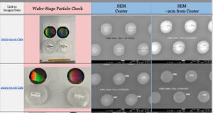
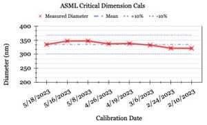
*''The Process Group regularly measures the lithography Critical Dimension ("CD") and Wafer-stage Particulate Contamination for this tool, using a sensitive lithography process that will reveal small changes in Dose repeatability and wafer flatness.'' |
|||
*[https://docs.google.com/spreadsheets/d/1xW1TFH_QjPMWl9T1jiKzwmYe4B2wg7KY-nqOKUoXttI/edit#gid=0 '''Data Table for CD Uniformity and Particulate Contamination'''] |
|||
*[https://docs.google.com/spreadsheets/d/1xW1TFH_QjPMWl9T1jiKzwmYe4B2wg7KY-nqOKUoXttI/edit#gid=1804752281 '''Plots of CD Repeatability'''] |
|||
{| |
|||
|[[File:ASML CD Cals - Example Table.jpg|alt=ASML CD Calibration data - Screenshot of Table|none|thumb|300x300px|''Example of Data Table with SEM's of 320nm features. [https://docs.google.com/spreadsheets/d/1xW1TFH_QjPMWl9T1jiKzwmYe4B2wg7KY-nqOKUoXttI/edit#gid=0 Click for full data table.]''|link=https://docs.google.com/spreadsheets/d/1xW1TFH_QjPMWl9T1jiKzwmYe4B2wg7KY-nqOKUoXttI/edit#gid=0]] |
|||
|[[File:ASML CD Cals - Example Plot.jpg|alt=ASML CD Calibration Data - Screenshot of SPC Plot|none|thumb|''Example SPC Chart - Measured Critical Dimension "CD" versus Date.'' ''[https://docs.google.com/spreadsheets/d/1xW1TFH_QjPMWl9T1jiKzwmYe4B2wg7KY-nqOKUoXttI/edit#gid=1804752281 Click for current charts.]''|link=https://docs.google.com/spreadsheets/d/1xW1TFH_QjPMWl9T1jiKzwmYe4B2wg7KY-nqOKUoXttI/edit#gid=1804752281]] |
|||
|} |
|||
<br /> |
|||
Latest revision as of 07:34, 10 April 2026
| ||||||||||||||||||||||||||||||||

| |
| |
| |
|
| |
| |
|
About
General Capabilities/Overview
The ASML 5500 stepper is a 248nm (KrF) DUV stepper for imaging dense features down to below 200nm and isolated line structures down to below 150nm (with effort). 300nm+ features are relatively "easy" to resolve. Layer-to-layer overlay accuracy is better than 30nm.
The system is configured for 4” wafers. The system is designed for high throughput, so shooting multiple 4" wafers is extremely fast, typically minutes per wafer, but any size other than 4-inch is difficult to work with (see below for more info). Additionally, exposure jobs are highly programmable, allowing for very flexible exposures of multiple aligned patterns from multiple masks/reticles in a single session, allowing for process optimization of large vs. small features in a single lithography.
The full field useable exposure area is limited to the intersection of a 31mm diameter circle and a rectangle of dimensions 22mm x 27mm. Users have stitched multiple photomasks together with success. See the Mask Making Guidelines page for more info on exposure field sizes and how to order your mask plates.
Stepper Tutorial
If you are not familiar with how Stepper Litho is different from our lithography methods, please review this short tutorial:
Stepper Reticle Layout vs Wafer Layout (Demis D. John) - Explains the following:
- That a Stepper mask layout is very different than other litho systems.
- That a Stepper mask can have many designs, and flexibly pattern the wafer with combos of designs.
Stepper Reticle Layout (Advanced) - Complex Experiments and Variations
- If you need many design variations on your wafer, this is an efficient way to utilize stepper reticles.
Photoresists Available
See PhotoLith. Recipes for full process info & links to PR datasheets.
- UV210-0.3 - Positive: 300nm nominal thickness
- UV6-0.8 - Positive: 800nm nominal thickness
- UV26-2.5 - Positive: 2.5um nominal thickness
- UVN2300-0.5 - Negative: 500nm nominal thickness
- DUV42P-6/DS-K101 - Bottom Anti-Reflective Coatings “BARC”
- PMGI/LOL1000/LOL2000 - Underlayers
AZ300MIF Developer for all processes
Many of these DUV PR's are also able to be exposed with EBL.
Part Size Limits
With staff support, mounted pieces down to 14mm in size can be exposed using a 4” wafer as a carrier. Flatness will typically be worse in this situation, so small <<500nm features will usually have bad uniformity across the mounted part due to focus variations. Edge bead on irregular pieces (eg. quarter-wafers/squares) will significantly reduce yield/uniformity.
Multi-layer Alignment on mounted parts is particularly difficult, requiring either semi-permanent mounting to the carrier (eg. BCB, SU8 etc.) or significant difficulty/effort to re-align the part to the carrier wafer on each lithography (≤100µm re-mounting accuracy needed).
At this time the maximum wafer size is 4” (100mm) wafers with SEMI standard wafer flat (not Notch).
Service Provider
- ASML - ASML performs quarterly periodic maintenance and provides on-demand support.
Process Information
- Process Recipes Page > "Stepper 3" - Established recipes and corresponding linewidths, photoresists etc.
- Sample size: 100 mm wafers with SEMI std. major flat
- Piece-parts process is possible but difficult - contact supervisor for info
- Alignment Accuracy: < 50 nm
- Minimum Feature Size: ≤150 nm isolated lines, ≤200 nm dense patterns
- To achieve ≤200nm features with high uniformity, we recommend wafers with total thickness variation (TTV) ≤5µm, and designing your CAD with a smaller Image Size for the high-res. feature.
- Wafer Thickness: Minimum ≈ 200µm, Maximum ≈ 1.1 mm
- Maximum Dose: ~100mJ
- Non-chemically amplified EBL resists are not permissible due to this limit.
Maximum Wafer Bow
Measured over 90mm on the Tencor Flexus
- Do not run wafers with bow values higher than the following values, contact supervisor for advice if needed.
- Silicon wafers (~550µm thick): 100 µm will likely fail.
- Sapphire (less pliable), ≥60µm bow will intermittently fail - DO NOT RUN
- This applies especially for GaN-on-Sapphire, which often have high wafer bow.
- Near these values, and you may lose the wafer inside the machine due to wafer vacuum error - DO NOT RUN if unsure.
- Substrate material and substrate thickness affect this limit - please contact supervisor for advice.
- You can stress-compensate wafers to reduce the wafer bow, eg. by depositing on the back side of the wafer. If your wafer is concave down, then depositing a compressive film on the back will reduce its curvature. Coat the backside of the wafer with compressive PECVD SiO2 or IBD SiN, or other compressive films for concave-down bow.
Operating Procedures
All procedures are access-restricted only to authorized users with a UCSB NetID (YourNetID@ucsb.edu), by vendor request.
Please contact supervisor for access/training.
ASML Operating Procedures
- Access-restricted google drive folder of PAS 5500/300 operating procedures.
Troubleshooting & Error Recovery
- common issues and fixes (access-restricted)
Calibrate Your Litho Process
See this section for the basics on how to do this: Stepper 3 (ASML DUV) > Recipes > Calibrating your Lithography Process
Stepper #3 Training/Reference Videos
- The above linked videos provide bookmarked quick-reference to various tool procedures & programming.
- To access, you must log in with your UCSB NetID, formatted like MyNetID@ucsb.edu - this is a Google login!
- Please contact the tool supervisor if you need access.
- Trouble accessing? Please click here for tips.
- You are NOT authorized to use this tool until a tool supervisor authorizes you!
Training Procedure
To get access to this tool, please do the following:
- Email the supervisor for access to the training materials. Please provide your UCSB NetID.
- Study the training videos.
- If you are a technician and will never program jobs, only Part 1 is necessary.
- "Shadow" someone in your group who uses the machine, until you are completely comfortable with (1) wafer cleaning (critical), (2) reticle load/unload and (3) running a pre-made job.
- When you are ready, request a hands-on check-off on SignupMonkey by clicking this button:
| Request Training |
|---|
Design Tools
Mask Design and CAD files
- Stepper Mask-Making Guidelines - Info needed to design and order a reticle for our Stepper systems. This is minimal unrestricted info that is viewable without additional paperwork.
- ASML-specific Mask Making Guidelines (Private) - More detailed info to design and order a reticle for this specific ASML system.
- Access is restricted to trained users only by ASML's requirement - please contact tool supervisor for access.
- Tutorial: Stepper Reticle Layout vs Wafer Layout (Demis D. John) - explains how Stepper mask layout is very different than other litho systems.
- Tutorial: Stepper Reticle Layout (Advanced) - Complex Experiments and Variations - If you need many design variations on your wafer.
- See the Calculators + Utilities > CAD Files & Templates page for other useful CAD files, such as overlay verniers, vented fonts etc.
UCSB Photomasks Available
- Click the above link to view our available masks & images
- Photomasks available with various patterns such as
- Alignment Markers (contact, EBL)
- Resolution Testing
- Various line/space (0.150µm → 50µm),
- Alignment markers modifications (dicing lane marks, rotated marks)
- Full-field exposure,
- 1mm boxes for LaserMonitor or Filmetrics/Dektak etc.
Optical Proximity Correction (OPC): Going below the resolution limit
- OPC General information and detailed investigation of lateral DBR patterns - Detailed info and investigation of OPC, use case examples, performance comparisons, how to order etc. By Gopikrishana G. Meena.
- UCSB Nanofab users have access to order photomask plates with OPC corrections applied to the patterns to enable accurate lithography on high-resolution structures, with a single photomask order.
- Model-based, "feed-forward" OPC - meaning you order only one photomask, no "feed-back", nor 2nd mask required.
- Photronics Inc. - OPC corrected mask plate provider for UCSB Nanofab users.
- Contact Demis for quotes.
- Photronics Inc. is collaborating with the Nanofab to develop + provide OPC correction to UCSB researchers.
- Photronics' team has built a model-based OPC correction for our system, which appears to work for multiple photoresists (UV6-positive and UVN-negative tested so far).
- Current OPC rules are for: Conventional (circular) Illumination / NA=0.57 / sigma=0.75
| OPC Mask Correction | Positive Resist: UV6-0.8 - Lateral Waveguide Gratings with/without OPC on same photomask.
Collaboration with photomask vendor Photronics Inc. | |
|---|---|---|

|

|

|
| OPC applies serifs to your patterns. | The Best exposure without OPC corrections; doesn't meet device criteria. Would require ordering a 2nd mask to correct. | With OPC applied to the patterns, the device criteria (length and spacing) are met on 1st mask rev, and process window is possibly wider. |
| Negative PR: UVN30. ASML DUV with and without same MB-OPC, on the same photomask, applied to a Meta-optic.
Fabricated by Skyler Palatnik, Prof. Max Millar-Blanchaer's group in collaboration with photomask vendor Photronics Inc. | |
|---|---|

|

|
| With OPC applied to mask pattern. Squares and circles with small gaps+small posts are resolved in one exposure. | Without OPC (standard photomask process). No combination of focus/dose can achieve desired results - "best" result shown here. |
JobCreator: Python Scripting
- Create ASML Job files using python. Click the above link for more info.
Recipes
- Recipes > Lithography > Stepper Recipes > Stepper #3 - starting processes for various DUV photoresists, including Dose/Focus values.
Calibrating your Lithography Process
To calibrate your own Litho processes, you will need to:
- Find a starter litho close to what you need here: Recipes > Lithography > Stepper Recipes > Stepper #3
- Run your own Focus Exposure Matrix with this procedure (private) - shows how to do an FEM on the ASML software
- Lithography Calibration - Analyzing a Focus-Exposure Matrix - how to analyze an FEM & choose the best process
Process Control Data
- The Process Group regularly measures the lithography Critical Dimension ("CD") and Wafer-stage Particulate Contamination for this tool, using a sensitive lithography process that will reveal small changes in Dose repeatability and wafer flatness.
- Data Table for CD Uniformity and Particulate Contamination
- Plots of CD Repeatability
 |
 |