Stepper Recipes: Difference between revisions
→Process Control Data: added particle check section and explanation/fig |
→Process Control Data: added thumbnail images of the Cals |
||
| Line 430: | Line 430: | ||
*[https://docs.google.com/spreadsheets/d/1xW1TFH_QjPMWl9T1jiKzwmYe4B2wg7KY-nqOKUoXttI/edit#gid=1804752281 '''Plots of CD Repeatability'''] |
*[https://docs.google.com/spreadsheets/d/1xW1TFH_QjPMWl9T1jiKzwmYe4B2wg7KY-nqOKUoXttI/edit#gid=1804752281 '''Plots of CD Repeatability'''] |
||
*[https://docs.google.com/spreadsheets/d/1xW1TFH_QjPMWl9T1jiKzwmYe4B2wg7KY-nqOKUoXttI/edit#gid=0 '''Data for CD Uniformity and Particulate Contamination'''] |
*[https://docs.google.com/spreadsheets/d/1xW1TFH_QjPMWl9T1jiKzwmYe4B2wg7KY-nqOKUoXttI/edit#gid=0 '''Data for CD Uniformity and Particulate Contamination'''] |
||
:{| |
|||
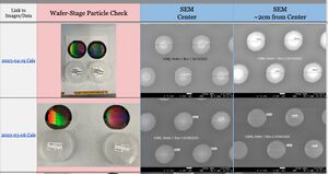
|[[File:ASML CD Cals - Example Table.jpg|alt=ASML CD Calibration data - Screenshot of Table|none|thumb|300x300px|''Example of Data Table with SEM's of 320nm features. [https://docs.google.com/spreadsheets/d/1xW1TFH_QjPMWl9T1jiKzwmYe4B2wg7KY-nqOKUoXttI/edit#gid=0 Click for full data table.]''|link=https://docs.google.com/spreadsheets/d/1xW1TFH_QjPMWl9T1jiKzwmYe4B2wg7KY-nqOKUoXttI/edit#gid=0]] |
|||
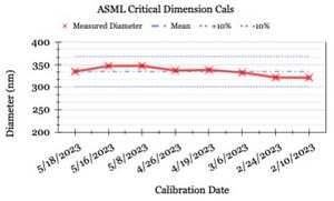
|[[File:ASML CD Cals - Example Plot.jpg|alt=ASML CD Calibration Data - Screenshot of SPC Plot|none|thumb|''Example SPC Chart - Measured Critical Dimension "CD" versus Date. [https://docs.google.com/spreadsheets/d/1xW1TFH_QjPMWl9T1jiKzwmYe4B2wg7KY-nqOKUoXttI/edit#gid=1804752281 Click for charts.]''|link=https://docs.google.com/spreadsheets/d/1xW1TFH_QjPMWl9T1jiKzwmYe4B2wg7KY-nqOKUoXttI/edit#gid=1804752281]] |
|||
|} |
|||
=== Particle Checks === |
=== Particle Checks === |
||
| Line 435: | Line 440: | ||
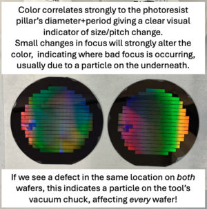
[[File:ASML Cal Particle Check.png|alt=Image showing 2 wafers with colorful rainbow patterns, both show a black spot on the right side.|none|thumb|Both wafers show a "hot spot" on the left side, so the tool has a particle at that location, requiring physical cleaning.]] |
[[File:ASML Cal Particle Check.png|alt=Image showing 2 wafers with colorful rainbow patterns, both show a black spot on the right side.|none|thumb|Both wafers show a "hot spot" on the left side, so the tool has a particle at that location, requiring physical cleaning.]] |
||
<br /> |
<br /> |
||
==Photomasks & Job Programming== |
==Photomasks & Job Programming== |
||
You can find info on making photomasks, CAD files for alignment marks, and other Job programming tools on the main Tool page, here: |
You can find info on making photomasks, CAD files for alignment marks, and other Job programming tools on the main Tool page, here: |
||
Revision as of 20:18, 16 July 2024
Back to Lithography Recipes.
Below is a listing of stepper lithography recipes. Stepper 1 and Stepper 2 are i-line systems with good piece handling capabilities. Stepper 3 is a DUV (248nm) system primarily used for full 100mm wafers. DUV resists do not work for i-line and i-line resists do not work for DUV. Based on your sample reflectivity, absorption (or whether or not you use an ARC layer), and surface topography, the exposure time / focus offset parameters may vary.
This listing is a guideline to get you started. For critical lithography steps, you should run your own exposure and/or focus array to determine the proper parameters.
The recipes are tabulated to give you the values of the key parameters you will need to establish your recipe. Underlayers such as LOL2000 or PMGI can be used on the stepper systems. See the underlayer datasheets for details. Post develop bakes (not listed) are used to make the resist more etch resistant and depend on subsequent processes. Care should be taken with post development bakes as resist reflow can occur. Unless otherwise noted, all exposures are done on flat, silicon wafers.
Parameters are indicated in separate tables for each stepper system.
Stepper 1 (GCA 6300)
Multiply the GCA 6300 exposure times by 0.30 to get a starting exposure time for the GCA Autostep200 system.
Positive Resist (GCA 6300)
Unless otherwise noted, bakes are on hot plates. For recipes with CEM, the CEM is spun on after the first resist bake, exposure is then done, and the CEM is rinsed off with DI water before the PEB. CEM generally improves resolution and process tolerance at the expense of higher exposure time.
| Resist | Spin Cond. | Bake | Thickness | Exposure Time | Focus Offset | PEB | Developer | Developer Time | Comments |
|---|---|---|---|---|---|---|---|---|---|
| SPR955CM0.9 | 3 krpm/30” | 95°C/60” | ~ 0.9 um | 1.2” | 0 | 110°C/60” | AZ300MIF | 60" |
|
| SPR955CM-0.9 | 3 krpm/30” | 95°C/60” | ~ 0.9 um | 3.0” | 4 | 110°C/60” | AZ300MIF | 60" |
|
| SPR955CM-0.9 |
3 krpm/30” 5 krpm/30” |
95°C/90” | ~ 0.9 um | 2.2” | -10 | 110°C/60” | AZ300MIF | 60" |
|
| SPR950-0.8 | 4 krpm/30” | 95°C/60” | ~ 0.8 um | 1.0” | 0 | 105°C/60” | AZ300MIF | 60" | |
| SPR955CM-1.8 | 4 krpm/30” | 90°C/90” | ~ 1.8 um | 2.3” | 0 | 110°C/90” | AZ300MIF | 60" |
|
| SPR955CM-1.8 | 4 krpm/30” | 90°C/90” | ~ 1.8 um | 1.7” | -5 | 110°C/90” | AZ300MIF | 60" |
|
| SPR220-3.0 | 2.5 krpm/30” | 115°C/90” | ~ 2.7 um | 2.4” | 10 | 115°C/90” | AZ300MIF | 60" |
|
| SPR220-7.0 | 3.5 krpm/45” | 115°C/120” | ~ 7.0 um | 4.5” | 0 | *50°C/60” 115°C/90” |
AZ300MIF | 120" |
|
Negative Resist (GCA 6300)
Unless otherwise noted, bakes are on hot plate. All flood exposures are done in broadband light using any contact aligner. Also, because the tone is negative, a shorter first exposure time will result in more undercut, which is desirable for single-layer lift-off processes. Under these conditions more develop time will also give more undercut.
| Resist | Spin Cond. | Bake | Thickness | Exposure Time | Focus Offset | PEB | Flood | Developer | Developer Time | Comments |
|---|---|---|---|---|---|---|---|---|---|---|
| AZ5214 | 6 krpm/30” | 95°C/60” | ~ 1.0 um | 0.2” | 0 | 110°C/60” | 60" | AZ300MIF | 60" |
|
| nLOF5510 | 3 krpm/30” | 90°C/60” | ~ 0.93 um | 0.74” | -6 | 110°C/60” | 0 | AZ300MIF | 60" |
|
| nLOF2020 | 4 krpm/30” | 110°C/60” | ~ 2 um | 0.55” | -6 | 110°C/60” | 0 | AZ300MIF | 90" |
|
Stepper 2 (AutoStep 200)
Positive Resist (AutoStep 200)
Unless otherwise noted, bakes are on hot plates. For recipes with CEM, the CEM is spun on after the first resist bake, exposure is then done, and the CEM is rinsed off with DI water before the PEB. CEM generally improves resolution and process tolerance at the expense of higher exposure time.
NOTE: The bolded exposure times were found by multiplying the exposure times from the GCA 6300 system by 0.30. They should be sued as a starting point. You will need to do an exposure array to get precise times for the Autostep system. In general, the resolution achievable is ~ 100 nm smaller for the Autostep200 system.
| Resist | Spin Cond. | Bake | Thickness | Exposure Time | Focus Offset | PEB | Developer | Developer Time | Comments |
|---|---|---|---|---|---|---|---|---|---|
| SPR955CM-0.9 | 3 krpm/30” | 95°C/90” | ~ 0.9 um | 0.35” | 0 | 110°C/90” | AZ300MIF | 60” |
|
| SPR955CM-0.9 | 3 krpm/30” | 95°C/90” | ~ 0.9 um | 0.8” | 0 | 110°C/90” | AZ300MIF | 60” |
|
| SPR955CM-1.8 | 4 krpm/30” | 95°C/90” | ~ 1.8 um | 0.4” | -1 | 110°C/90” | AZ300MIF | 60” | |
| SPR950-0.8 | 4 krpm/30” | 95°C/60” | ~ 0.8 um | 0.30” | 0 | 105°C/60” | AZ300MIF | 60" | |
| SPR220-3.0 | 2.5 krpm/30” | 115°C/90” | ~ 2.7 um | 0.72” | 10 | 115°C/90” | AZ300MIF | 60" |
|
| SPR220-7.0 | 3.5 krpm/45” | 115°C/120” | ~ 7.0 um | 1.35" | 0 | *50°C/60” 115°C/90” |
AZ300MIF | 120" |
|
| AZ4210 | step1:500rpm/5", step2:4krpm/45” | 95°C/60" | ~ 2.1 um | 0.75" | 0 | AZ400K:DI=1:4 | 60" |
|
Negative Resist (AutoStep 200)
Unless otherwise noted, bakes are on hot plate. All flood exposures are done in broadband light using any contact aligner. Also, because the tone is negative, a shorter first exposure time will result in more undercut, which is desirable for single-layer lift-off processes. Under these conditions more develop time will also give more undercut.
NOTE: The bolded exposure times were found by multiplying the exposure times from the GCA 6300 system by 0.30. They should be sued as a starting point. You will need to do an exposure array to get precise times for the Autostep system. In general, the resolution achievable is ~ 100 nm smaller for the Autostep200 system.
| Resist | Spin Cond. | Bake | Thickness | Exposure Time | Focus Offset | PEB | Flood | Developer | Developer Time | Comments |
|---|---|---|---|---|---|---|---|---|---|---|
| nLOF5510 | 3 krpm/30” | 90°C/60” | ~ 0.93 um | .25” | -1 | 110°C/60” | 0 | AZ300MIF | 60” |
|
| AZ5214 | 6 krpm/30” | 95°C/60” | ~ 1.0 um | 0.06” | 0 | 110°C/60” | 60" | AZ300MIF | 60" |
|
| nLOF2020 | 4 krpm/30” | 110°C/60” | ~ 2 um | 0.17” | -6 | 110°C/60” | 0 | AZ300MIF | 90" |
|
| NR9-1000PY | 3 krpm/30” | 135°C/180” lid down | ~ 1.2 um | 0.92” | 0 | 115°C/120” lid down | 0 | AZ300MIF | 20" |
|
Stepper 3 (ASML DUV)
| Stepper 3: Table of Contents |
|---|
|
Process Control Data
- The Process Group regularly measures data on lithography Critical Dimension ("CD") and Wafer-stage Particulate Contamination for this tool, using a sensitive lithography process that will reveal small changes in Dose repeatability and wafer flatness.
- Plots of CD Repeatability
- Data for CD Uniformity and Particulate Contamination

Example of Data Table with SEM's of 320nm features. Click for full data table. 
Example SPC Chart - Measured Critical Dimension "CD" versus Date. Click for charts.
Particle Checks
Our cal process enables both ~300nm critical dimension logging, and also allows us to see when a particle is present on the exposure chuck (a "hot spot").

Photomasks & Job Programming
You can find info on making photomasks, CAD files for alignment marks, and other Job programming tools on the main Tool page, here:
Stepper 3 (ASML DUV) > Design Tools
Anti-Reflective Coatings
Bottom Anti-reflective coatings (aka. BARC or AR Coating) are, in general, used for the ASML stepper. LOL2000 and PMGI can also be used as under layers. BARC layers will increase the process tolerance, especially for features ≤ wavelength (248nm).
For example, without BARC you might find that 200nm features only resolve with focus of -0.2µm to -0.3µm, while with BARC the process tolerance may increase to -0.1µm to -0.4µm, which also increases tolerance to wafer flatness/PR spin uniformity.
DUV-42P-6
(replacement for AR2)
- spin coat at 2500rpm for optimal anti-reflective properties (~60nm).
- Mistake: this was previously written as 3500rpm.
- Bake at 220°C for 60s on a hotplate.
- This AR coating is removed via oxygen plasma.
- This ARC can be etched on ICP#1, ICP#2, RIE#5, FL-ICP or even Technics PEii ashers.
- Datasheet: DUV-42P-6
DS-K101-304
- Spin at 1500rpm and bake at 185°C for 60sec
- Approx 40nm for best anti-reflective properties
- Mistake: previously written as 5000rpm, ~20nm thickness (from DS-K101-307)
- This AR coating develops away and undercuts in AZ300MIF.
- For isolated lines, this can cause them to lift-off by undercutting the resist.
- Increase bake temperature to reduce undercut rate.
- DS-K101-304 Bake Temp. versus Develop Rate - Click for experimental data
- Can be used similarly to DUV42P (dry etch removal) by baking at 220°C.
- Datasheet: DS-K101-304
Positive Resist (ASML DUV)
Please see section above for anti-reflection coatings, which are usually used with the DUV Stepper.
| Resist | Spin Cond. | Bake | Thickness | Exposure Dose(mj) | Focus Offset | PEB | Developer | Developer Time | Comments |
|---|---|---|---|---|---|---|---|---|---|
| UV6-0.7 (replaced by UV6-0.8) |
3.5 krpm/30” | 135°C/60” | 630nm | 17 | -0.2 | 135°C/90” | AZ300MIF | 45” |
|
| UV210-0.3 | 5.0 krpm/30” | 135°C/60” | 230nm | 20 | -0.1 | 135°C/90” | AZ300MIF | 45" |
|
| UV210-0.3 | 3.0 krpm/30” | 135°C/90” | 260nm | 85 | -0.2 | 135°C/90” | AZ300MIF | 80” |
|
| UV26-2.5 | Available but no recipes characterized | 135°C/90s | ~2.5 µm | approx. 40 | approx. +0.8 | 110°C/90s | AZ300MiF | Unknown | Users must run your own development/FEM's. |
Negative Resist (ASML DUV)
Please see section above for anti-reflection coatings, which are usually used with the DUV Stepper.
| Resist | Spin Cond. | Bake | Thickness | Exposure Dose (mj) | Focus Offset | PEB | Flood | Developer | Developer Time | Comments |
|---|---|---|---|---|---|---|---|---|---|---|
| UVN30-0.8 | 3.5 krpm/30” | 110°C/60” | ~550nm | 27 | +0.15 | 105°C/60” | Not Used | AZ300MIF | Approx. 20sec
(not thoroughly calibrated) |
|