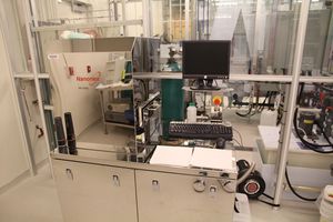
Nano-Imprint (Nanonex NX2000)
|
About
The Nanonex NX2000 is a nanoimprinting system that allows for direct pattern transfer from a pre-fabricated master mold into an underlying polymer material. Lateral feature sizes down to less than 10 nm have been demonstrated on this tool. The system can do thermal imprinting into a polymer at temperatures up to 200°C and chamber pressures up to 600 psi. The system can also imprint into and cure UV-cureable materials on top of underlayer polymers in order to planarize samples and provide for high aspect ratio imprint lithography. Since the system uses no rigid plates, but air pressure only, the pressure uniformity is excellent in the system. The heating and cooling rates are as high as 300°C/min. Several types of resists are supplied, including NXR-1020, mr-l-7020, and MR-UVCur21. The system is capable of handling piece parts up to 100 mm wafers. An additional alignment system is also available for 100 mm wafers for aligned imprinting. Non-stick coatings for master molds are deposited using FDTS in the Molecular Vapor Deposition system. For creation of master molds, please call for a discussion of our other capabilities, including electron-beam lithography.
Detailed Specifications
- Thermal imprinting up to 200°C and 600 psi chamber pressure (equivalent to 1200 psi on the wafer stack); 300°C/min heat-cool rates
- UV-imprinting
- In-house resist processes and subsequent pattern transfer offered
- Resolution: 10 nm demonstrated
- Minimum substrate size: small pieces
- Largest substrate size: 100 mm wafer
- Several resists, non-stick layers, and master copy formation also available.
