Tutorials: Difference between revisions
Jump to navigation
Jump to search
Content deleted Content added
pasted lins to various mask palges across the wiki |
|||
| (13 intermediate revisions by the same user not shown) | |||
| Line 1: | Line 1: | ||
The following are various tutorials from our NanoFab Wiki, collected here for your convenience. |
|||
| ⚫ | |||
__TOC__ |
|||
| ⚫ | |||
:[[File:CAD Tutorial for ASML Reticle v1 - screenshot Device Layout cell.png|alt=screenshot of KLayout view of Device_Layout|thumb|300x300px|KLayout: example CAD file.]] |
|||
== General Fabrication == |
|||
* [[Processing - How Do I…?]] ← This page attempts to list common solutions to fabrication issues our lab users often run into. |
|||
* [https://drive.google.com/file/d/1B-Xg254T-RdALisnms0jvpJQ34i5TNXN/view Design of Experiments: Taguchi/L9 DOE methods] - [[Gopikrishnan G M|Gopi]] explains how to identify trends in your process, using multi-variable experiments (to minimize the number of experiments). Do this when you don't have a good physical understanding of how the process variables interact. |
|||
== Fabrication Tracking and Process Design == |
|||
Designing experiments, tracking your fabrication steps/process improvements, and keeping track of your results are key to achieving repeatable and improved results! |
|||
[[Processing - How Do I…?#Experiment%20Setup|<big>'''Processing: Experiment Setup'''</big>]] |
|||
See the above ↑ tutorial pages for examples of: |
|||
* [[Processing - How Do I…?#Travelers (aka. RunCards, Process Followers, Work Instructions)|Process Travelers/RunCards/Followers]] - ''Write your process and track what you <u>actually</u> did during the fab'' |
|||
* [[Processing - How Do I…?#Design of Experiments (DOE)|Design of Experiments]] - ''Develop/optimize a fab step'' |
|||
* [[Processing - How Do I…?#Tracking your processes|Manufacturing Execution Systems]] - ''Track all your designs, fab runs and experiment results, so you can iterate.'' |
|||
{| class="wikitable" |
|||
|+Examples of Trello + Google Drive for tracking fabrication jobs |
|||
|[[File:Trello - Example Job Cards.png|alt=Trello - Example Job Cards screenshot|none|thumb|367x367px|Tracking to-do and completed tasks.]][[File:Google Drive - Example Job Folder.png|alt=Google Drive - Example Job Folder screenshot|none|thumb|327x327px|Example Job Folder on Google Drive with in-process traveler, microscope/SEM images, testing results etc.]] |
|||
|[[File:Trello - example job card.png|alt=Trello - example job card screenshot|none|thumb|504x504px|Example job card for a fabrication run.]] |
|||
|} |
|||
| ⚫ | |||
| ⚫ | :Here are pages to help you design your devices in drawing programs, and make photomasks (aka. "masks" or "reticles") for various systems in our lab.[[File:CAD Tutorial for ASML Reticle v1 - screenshot Device Layout cell.png|alt=screenshot of KLayout view of Device_Layout|thumb|300x300px|KLayout: example CAD file.]] |
||
Microfabrication CAD drawings are simple 2D drawings with layers, even though they are intended to become 3D devices through the fabrication process. The fabrication is all top-down, hence only 2D patterning is used. |
Microfabrication CAD drawings are simple 2D drawings with layers, even though they are intended to become 3D devices through the fabrication process. The fabrication is all top-down, hence only 2D patterning is used. |
||
| Line 10: | Line 33: | ||
* [[Calculators + Utilities#CAD%20Files%20%26%20Templates|Calculators + Utilities > CAD Files & Templates]] - example GDS/OAS files for various useful structures (alignment marks, verniers, fonts etc) |
* [[Calculators + Utilities#CAD%20Files%20%26%20Templates|Calculators + Utilities > CAD Files & Templates]] - example GDS/OAS files for various useful structures (alignment marks, verniers, fonts etc) |
||
== |
== Mask Making Guidelines == |
||
''Info for mask/CAD layout for specific tools.'' |
|||
==== General ==== |
|||
| ⚫ | |||
* See [[Tutorials#CAD/Drawing Mask Plates|CAD tutorials above]] for layout tips and examples. |
|||
* [[Tutorial - How Photomasks are Made]] - this will help you submit your mask orders and clear up common misconceptions. |
|||
==== Stepper Mask Tutorials ==== |
|||
[[File:Stepper Reticle Tutorial - Reticle Masking Schematic.png|alt=Schematic of stepper blocking off adjacent Images on reticle and exposure onto different wafer locations.|thumb|'''[https://wiki.nanofab.ucsb.edu/w/images/c/cb/Demis_D_John_-_Stepper_Reticle_Layout_vs_Wafer_Layout.pdf Click for Stepper Reticle Tutorial]''' Stepper Reticle Patterns (“images”) can optionally be much more sophisticated and flexible than contact plates.|link=https://wiki.nanofab.ucsb.edu/w/images/c/cb/Demis_D_John_-_Stepper_Reticle_Layout_vs_Wafer_Layout.pdf]] |
[[File:Stepper Reticle Tutorial - Reticle Masking Schematic.png|alt=Schematic of stepper blocking off adjacent Images on reticle and exposure onto different wafer locations.|thumb|'''[https://wiki.nanofab.ucsb.edu/w/images/c/cb/Demis_D_John_-_Stepper_Reticle_Layout_vs_Wafer_Layout.pdf Click for Stepper Reticle Tutorial]''' Stepper Reticle Patterns (“images”) can optionally be much more sophisticated and flexible than contact plates.|link=https://wiki.nanofab.ucsb.edu/w/images/c/cb/Demis_D_John_-_Stepper_Reticle_Layout_vs_Wafer_Layout.pdf]] |
||
| Line 16: | Line 47: | ||
* '''[[Stepper Reticle Layout (Advanced) - Complex Experiments and Variations]]''' - If you need many design variations on your wafer. |
* '''[[Stepper Reticle Layout (Advanced) - Complex Experiments and Variations]]''' - If you need many design variations on your wafer. |
||
==== Steppers ==== |
|||
== Mask Making Guidelines == |
|||
| ⚫ | |||
| ⚫ | |||
| ⚫ | |||
| ⚫ | |||
| ⚫ | |||
** ''Access is restricted to trained users only by ASML's requirement - please contact [[Demis D. John|tool supervisor]] for access.'' |
** ''Access is restricted to trained users only by ASML's requirement - please contact [[Demis D. John|tool supervisor]] for access.'' |
||
* [[Autostep 200 Mask Making Guidance]] - information on designing and ordering your photomasks for the GCA AutoStep 200. |
* [[Autostep 200 Mask Making Guidance]] - information on designing and ordering your photomasks for the GCA AutoStep 200. |
||
* [[GCA 6300 Mask Making Guidance]] (''Work in progress'') - GCA 6300 Stepper |
* [[GCA 6300 Mask Making Guidance]] (''Work in progress'') - GCA 6300 Stepper |
||
==== Contact Aligners ==== |
|||
* [[Mask Making Guidelines for Contact Aligners|Mask Making Guidelines - Contact Masks]] - for the MJB-3 & MA6 Contact Aligners |
* [[Mask Making Guidelines for Contact Aligners|Mask Making Guidelines - Contact Masks]] - for the MJB-3 & MA6 Contact Aligners |
||
| ⚫ | |||
==== Direct-Write ==== |
|||
Projection litho systems (steppers, direct-writers) usually require a lithography calibration, as follows: |
|||
| ⚫ | |||
== Lithography Tutorials == |
|||
* [[Lithography Calibration - Analyzing a Focus-Exposure Matrix|Lithography Calibration - Analyzing a Focus-Exposure Matrix (FEM)]] - |
* [[Lithography Calibration - Analyzing a Focus-Exposure Matrix|Lithography Calibration - Analyzing a Focus-Exposure Matrix (FEM)]] - Projection litho systems (steppers, direct-writers) usually require a lithography calibration, using a Focus-Exposure Matrix/Array (FEM/FEA). |
||
*{{fl|Liftoff-Techniques.pdf|Lift-Off Description/Tutorial}} - How it works, process limits and considerations for designing your process. |
|||
Latest revision as of 01:29, 13 June 2026
The following are various tutorials from our NanoFab Wiki, collected here for your convenience.
General Fabrication
- Processing - How Do I…? ← This page attempts to list common solutions to fabrication issues our lab users often run into.
- Design of Experiments: Taguchi/L9 DOE methods - Gopi explains how to identify trends in your process, using multi-variable experiments (to minimize the number of experiments). Do this when you don't have a good physical understanding of how the process variables interact.
Fabrication Tracking and Process Design
Designing experiments, tracking your fabrication steps/process improvements, and keeping track of your results are key to achieving repeatable and improved results!
See the above ↑ tutorial pages for examples of:
- Process Travelers/RunCards/Followers - Write your process and track what you actually did during the fab
- Design of Experiments - Develop/optimize a fab step
- Manufacturing Execution Systems - Track all your designs, fab runs and experiment results, so you can iterate.
  |
 |
CAD/Drawing Mask Plates
- Here are pages to help you design your devices in drawing programs, and make photomasks (aka. "masks" or "reticles") for various systems in our lab.
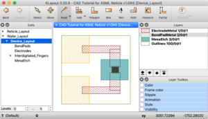
KLayout: example CAD file.

Microfabrication CAD drawings are simple 2D drawings with layers, even though they are intended to become 3D devices through the fabrication process. The fabrication is all top-down, hence only 2D patterning is used.
- Calculators + Utilities > CAD Layout and Mask Design - links to drawing programs and tutorials
- Calculators + Utilities > CAD Design Tips - key concepts you should utilize in your drawings, and tips for setting up your CAD programs
- Calculators + Utilities > Example CAD File - example stepper mask CAD files, including advanced layout for multiple experiments.
- Calculators + Utilities > CAD Files & Templates - example GDS/OAS files for various useful structures (alignment marks, verniers, fonts etc)
Mask Making Guidelines
Info for mask/CAD layout for specific tools.
General
- Photomask Ordering Procedure for UCSB Users - see this page for how to submit your order into the purchasing system.
- See CAD tutorials above for layout tips and examples.
- Tutorial - How Photomasks are Made - this will help you submit your mask orders and clear up common misconceptions.
Stepper Mask Tutorials
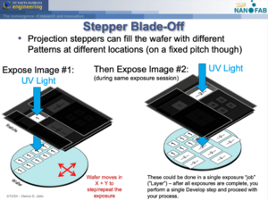
- Stepper Reticle Layout vs Wafer Layout (Demis D. John) - explains how Stepper mask layout is very different than other litho systems.
- Stepper Reticle Layout (Advanced) - Complex Experiments and Variations - If you need many design variations on your wafer.
Steppers
- Stepper Mask-Making Guidelines - Info needed to design and order a reticle for our Stepper systems.
- ASML-specific Mask Making Guidelines (Private) - More detailed info to design and order a reticle for this specific ASML system.
- Access is restricted to trained users only by ASML's requirement - please contact tool supervisor for access.
- Autostep 200 Mask Making Guidance - information on designing and ordering your photomasks for the GCA AutoStep 200.
- GCA 6300 Mask Making Guidance (Work in progress) - GCA 6300 Stepper
Contact Aligners
- Mask Making Guidelines - Contact Masks - for the MJB-3 & MA6 Contact Aligners
Direct-Write
- MLA150 - Design Guidelines - for the Heidelberg MLA150 Direct-Writer
Lithography Tutorials
- Lithography Calibration - Analyzing a Focus-Exposure Matrix (FEM) - Projection litho systems (steppers, direct-writers) usually require a lithography calibration, using a Focus-Exposure Matrix/Array (FEM/FEA).
- Lift-Off Description/Tutorial - How it works, process limits and considerations for designing your process.