SEM 1 (JEOL IT800SHL): Difference between revisions
mentioned nabity litho |
|||
| Line 20: | Line 20: | ||
The [[SEM Sample Coater (Hummer)|'''<u>Hummer coater</u>''']] is used to deposit a thin AuPd on your samples, to reduce electrical charging of insulating samples (such as SiO2 substrates, or thick >1µm layers of SiO2 or PR). |
The [[SEM Sample Coater (Hummer)|'''<u>Hummer coater</u>''']] is used to deposit a thin AuPd on your samples, to reduce electrical charging of insulating samples (such as SiO2 substrates, or thick >1µm layers of SiO2 or PR). |
||
This SEM also has an Electron-Beam Lithography Nabity system. Contact the supervisor for info. |
|||
==Detailed Specifications== |
==Detailed Specifications== |
||
| Line 54: | Line 56: | ||
**max: 70 x 50mm |
**max: 70 x 50mm |
||
**4-inch wafer: limited to ~25x25mm movement area from wafer center. |
**4-inch wafer: limited to ~25x25mm movement area from wafer center. |
||
*Tilt: -5° to varies. Tilt is dependent on sample holder, stage height, and offset value. |
*Tilt: -5° to varies. Tilt is dependent on sample holder, stage height, and offset value. |
||
*Rotation: 360° |
*Rotation: 360° |
||
*Specimen holders : |
*Specimen holders : |
||
Revision as of 19:10, 23 February 2024
| ||||||||||||||||||||||||||
About
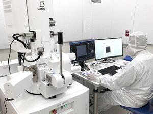
The JEOL IT800HSL Field Emission Scanning Electron Microscope is used for imaging a variety of samples made in the facility.
Capabilities
The system has multiple detectors, detailed below. Low-vacuum mode reduces sample charging by introducing N2 gas into the chamber, without sacrificing imaging quality (using a special vacuum nozzle on the electron column). Our system is equipped with a gentle-beam mode of operation where bias is put on the stage, allowing for high resolution imaging at low electron energies impinging the surface. Both of these are useful for imaging low conductivity and insulating materials without the need for conductive layer coatings.
The system can accept a 6” wafer, but only XYZXYZ mm of the wafer is accessible with the stage movement.
The Hummer coater is used to deposit a thin AuPd on your samples, to reduce electrical charging of insulating samples (such as SiO2 substrates, or thick >1µm layers of SiO2 or PR).
This SEM also has an Electron-Beam Lithography Nabity system. Contact the supervisor for info.
Detailed Specifications
Imaging
- Resolution:
- 1nm guaranteed at 15kV SEM mode
- 2.5nm at 1kV in SEM mode
- 1.5nm at 1kV in GB mode
- Magnification:
- SEM: x100 (at WD 25mm) to x1,000,000 (at WD 8mm)
- Low-Mag LM mode: x25 to x19,000
- Imaging Modes/Detectors:
- SEI: secondary electron imaging
- LM: Low-magnification mode
- GB: Gentle-Beam mode
- Applies negative voltage to sample stage to increase effective acceleration without increasing beam acceleration (reducing charging).
- LABE: Low-Angle Backscatter Electron detector
- Inserts between the objective lens and the sample
- Strong contrast between materials
- LEI: Lower Electron Detector
- Detector is lower on chamber, creating strong topographical contrast.
- Accelerating Voltages:
- SEM: 0.5 to 30kV
- GB: 0.1 to 4.0kV
- Beam Currents: 10-13 to 2x10⁻⁷ A
Mechanical
- Max Sample Size: 6-inch wafer
- Stage movement:
- max: 70 x 50mm
- 4-inch wafer: limited to ~25x25mm movement area from wafer center.
- Tilt: -5° to varies. Tilt is dependent on sample holder, stage height, and offset value.
- Rotation: 360°
- Specimen holders :
- Copper and XYZ Carbon tape available
- 4-inch wafer with topside clips
- 1-inch holder for 30°/90°, 45°/90° mounting with tape or clips.
