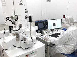
SEM 1 (JEOL IT800SHL): Difference between revisions
→Operating Procedures: link to hummer techniques |
→Operating Procedures: link to reduced cahrging imaging modes page |
||
| Line 60: | Line 60: | ||
==Operating Procedures== |
==Operating Procedures== |
||
* |
*[https://wiki.nanofab.ucsb.edu/w/images/1/10/JEOL_IT800SHL_Operating_Procedure.docx JEOL IT800SHL Operating Procedure]. |
||
*[https://www.youtube.com/watch?v=YeukVt1Fyi0 Optimizing Astigmatism (CalTech Nanoscience Institute)] |
*[https://www.youtube.com/watch?v=YeukVt1Fyi0 Optimizing Astigmatism (CalTech Nanoscience Institute)] |
||
**Stig is the most common cause of blurry images, and requires practice to improve/knowing what to look for. |
**Stig is the most common cause of blurry images, and requires practice to improve/knowing what to look for. |
||
**A Common mistake is to optimize stig on flat lines (eg. a cleaved edge or line/space features). This always leads to accidentally skewing the stig in the direction of the lines. Instead, make sure to optimize on a roundish feature, such as a piece of dust/debris. |
**A Common mistake is to optimize stig on flat lines (eg. a cleaved edge or line/space features). This always leads to accidentally skewing the stig in the direction of the lines. Instead, make sure to optimize on a roundish feature, such as a piece of dust/debris. |
||
*[[Hummer SEM Sample Coater - Techniques to reduce charging in SEMs]] |
*[[Hummer SEM Sample Coater - Techniques to reduce charging in SEMs|Hummer SEM Sample Coater - thin Au/Pd coating to reduce charging in SEMs]] |
||
*[[JEOL IT800SHL - Reduced Charging Imaging Modes|Charge-Free Imaging]] - SEM settings to reduce charging during imaging. |
|||
Revision as of 16:41, 2 November 2024
| ||||||||||||||||||||||||||
About
The JEOL IT800HSL Field Emission Scanning Electron Microscope is used for imaging a variety of samples made in the facility.
Capabilities
The system has multiple detectors, detailed below. Low-vacuum mode reduces sample charging by introducing N2 gas into the chamber, without sacrificing imaging quality (using a special vacuum nozzle on the electron column). Both of these are useful for imaging low conductivity and insulating materials without the need for conductive layer coatings.
The system can accept a 6” wafer, but only 140mm (X) and 80mm (Y) of the wafer is accessible with the stage movement.
The Hummer coater is used to deposit a thin AuPd on your samples, to reduce electrical charging of insulating samples (such as SiO2 substrates, or thick >1µm layers of SiO2 or PR).
This SEM also has an Electron-Beam Lithography Nabity system. Contact Aidan Hopkins for info.
Detailed Specifications
Imaging
- Resolution:
- 0.5nm at 15kV SHL mode
- 0.7nm at 1kV
- 0.9nm at 500V
- Magnification:
- Photo magnification: x10 to x2,000,000 (128mm x 96mm)
- Display magnification: x27 to x5,480,000 (1280pix x 960pix)
- Imaging Modes:
- STD: Standard
- LDF: Large depth of focus
- BD: Beam deceleration
- Applies negative voltage to sample stage to increase effective acceleration without increasing beam acceleration (reducing charging).
- SHL: Super hybrid lens ("immersion" lens)
- Detectors
- SED: Secondary electron detector (low angle) - default
- UHD: Ultra high resolution detector
- SBED: Scintillated back scatter electron detector
- Inserts between the objective lens and the sample, high Z-contrast
- LVBED: Low vacuum back scatter electron detector
- LVSED: Low vacuum secondary electron detector
- Accelerating Voltages:
- SEM: 0.01 to 30kV
- Probe currents
- A few pA to 500nA (30kV) 100nA (5kV)
- Specimen stage
- X: 140mm Y: 80mm
- Z: 6mm to 41mm
- Tilt: -5 to 70 degrees (depending on sample holder and offset)
- Rotation: 360 degrees
Operating Procedures
- JEOL IT800SHL Operating Procedure.
- Optimizing Astigmatism (CalTech Nanoscience Institute)
- Stig is the most common cause of blurry images, and requires practice to improve/knowing what to look for.
- A Common mistake is to optimize stig on flat lines (eg. a cleaved edge or line/space features). This always leads to accidentally skewing the stig in the direction of the lines. Instead, make sure to optimize on a roundish feature, such as a piece of dust/debris.
- Hummer SEM Sample Coater - thin Au/Pd coating to reduce charging in SEMs
- Charge-Free Imaging - SEM settings to reduce charging during imaging.
